Printed circuit boards (PCBs) form the backbone of electronics. Understanding the PCB fabrication process helps appreciate the precision and intricacy involved in reliably mass producing these wired boards. This guide takes you step-by-step through the key PCB manufacturing stages along with tips for ensuring optimal quality.
Overview of the PCB Manufacturing Process
The PCB fabrication process consists of:
- Design and Layout
- Prototype Iterations
- Producing Fabrication Data
- Substrate Selection
- Lamination
- Drilling
- Metallization
- Photolithography
- Etching
- Soldermask Application
- Silkscreen Printing
- Surface Finishes
- Electrical Testing
- Final Quality Inspection
- Panelization
- Shipment
Now let’s delve into the nitty-gritty details of each step:
1. Design and Layout
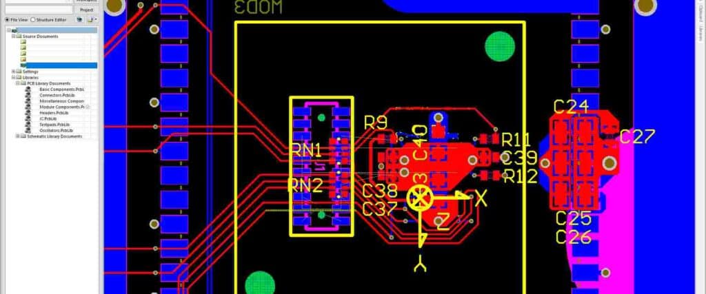
PCB fabrication begins on the computer using electronic design automation (EDA) software like OrCAD, Altium, Eagle etc. The board circuitry layout will depend on complexity of connections, component selection, form factor constraints and performance requirements.
Key layout considerations impacting board fabrication:
Trace widths – Match with current levels handled. Thicker traces used for higher current capacity.
Spacing constraints – Closer spacing for denser designs but ensure no short circuits.
Number of layers – Stacked layers accommodate complex designs. But more layers increase fabrication costs.
Via styles – Blind, buried or through-hole vias offer routing flexibility. But can impact drilling, metallization, costs.
Controlled Impedance – Match trace widths and dielectric spacing to achieve target impedance matching for high frequency or rise time sensitive signals.
Plane layers – Uninterrupted copper layers enhance power distribution and shields noise in multilayer boards.
Durability – Environmental operating conditions dictate board finishes, protective coatings.
Testability – Incorporate test points for validation and troubleshooting.
The completed board layouts consisting of traces, pads, vias and holes is thoroughly verified in the CAD tool before releasing the data package for fabrication.
2. Prototype Iterations
It’s prudent to build a prototype version first and test key functionality before committing to full production. This offers chance to tweak design issues missed during layout review.
For prototypes, only a few PCBs are fabricated without advanced automation to keep costs low. If no showstopper issues are unearthed, one can proceed to final fabrication build.
3. Producing Fabrication Data
The PCB layout data must be converted into format compatible with fabrication equipment. This process data includes:
Gerber files – Contains circuit copper layers, solder masks, legend, drill data etc. as individual images. Becomes printer input.
Excellon Drill files – Specifies drill sizes and hole coordinates. Guides automated drilling machines.
Netlist – Matches component pads with signals in schema for testing assembled boards.
Assembly Drawings – Diagrams for population reference during component assembly.
Bill of Materials (BOM) – Lists all components with reference designators, manufacturer part numbers, quantity.
The Gerber data undergoes final checks for errors using validation tools before release.
4. Substrate Selection
The PCB fabrication begins by selecting a suitable insulating substrate material to build up the conductive copper layers. Some options:
FR-4 Glass Epoxy – Most common rigid fiberglass reinforced epoxy resin sheets. FR-4 glass woven material imparts mechanical strength. Flame retardant grade.
CEM-1 Cotton Paper – Woven cellulose cotton paper bonded with epoxy resin. Excellent high frequency performance. Costlier than FR-4.
Rogers Laminates – High frequency boards with precise dielectric constant and low loss tangent. Expensive but tightly controlled electrical performance.
Flexible Films – Polyimide, polyester, Teflon flexible circuit materials for bending applications. Polyimide can withstand soldering temperatures.
Aluminum Boards – Metal core boards directly bond copper foil onto aluminum substrate without dielectric in between. Excellent thermal performance.
Ceramic Boards – Alumina ceramic substrate has superior thermal performance but very brittle. Used only for niche applications.
The substrate parameters like glass transition temperature, CTE coefficient, flexural strength, thermal conductivity etc. decides PCB fabrication process compatibility.
5. Lamination
The core substrate must now be prepared for layer buildup by bonding thin sheets of copper foil onto one or both sides. This lamination process involves:
Surface Preparation – Substrate sheets undergo chemical or mechanical processes to roughen surface and improve copper foil adhesion.
Foil Application – Rolls of thin copper foil, either electrodeposited or rolled, get attached to core substrate sheet under high pressure and temperature. The resin system cures bonding foil firmly.
Cooling – The laminated sheets are cooled under controlled tension to prevent wrinkling before proceeding to next steps.
For multi-layer boards, layers of prepreg bonding sheet and copper foil are stacked up into a book before undergoing high pressure fusion lamination. This allows building multilayer sandwich with copper layers interconnected through plated through holes.
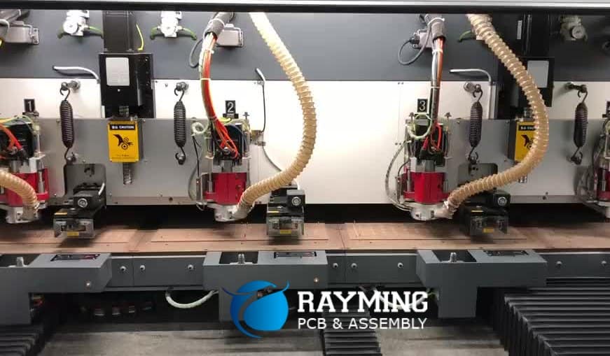
6. Drilling
Laminated boards undergo drilling operation to bore holes that create vias for vertical interconnection of layers and component holes for leads to pass through. Some key drilling aspects:
CNC Drills – Computer numerical controlled (CNC) drilling machines use Excellon file input to accurately drill thousands of holes. Multi-spindle drills can work on multiple boards for high productivity.
Hole Wall Quality – The drilling parameters are optimized to ensure no rough edges, burrs or copper smearing. This allows clean copper plating inside walls.
Hole Size Tolerances – Drill bits wear out so they need frequent sharpening and replacement to maintain tight size variations.
Registration Accuracy – Precision drilling fixtures align boards so vias land accurately on inner layer pads without offset errors.
Deburring – Boards get routed to deburring station to clean up any miniature copper burrs or particles using small abrasive brushes or chemical process.
Depth Control – Multi-layer boards need different hole depths. So drill press height gets adjusted during depth transitions.
Panelization – Individual PCB units get framed into larger panels for mass drilling followed by later singulation.
Lamination Cleanup – Post drilling, the panel edges get trimmed to remove extraneous lamination material.
7. Metallization – Copper Plating
To allow electrical connectivity through the freshly drilled holes, their insulating walls need metallic coating. This is achieved by copper electroplating process:
Desmear – The hole walls get micro-etched to remove resin smear and expose glass fiber mesh for improved plating adhesion.
Activation – A sensitizer like palladium chloride prepares hole surfaces for initiating copper deposition during plating by catalyzing reactive sites.
Electroless Copper – First a thin layer of copper gets auto-catalytically deposited without any external current to form base layer.
Electrolytic Copper – Thicker copper layer gets built up by electroplating using external DC current via submerged conductive anodes and board acting as cathode. Uniform thickness achieved despite challenging hole geometry.
Plugging – All holes get fully plugged flush with copper yielding a continuous conductive surface.
For multilayer boards, this copper plating electrically interconnects the inner layer pads through the plated hole barrels.
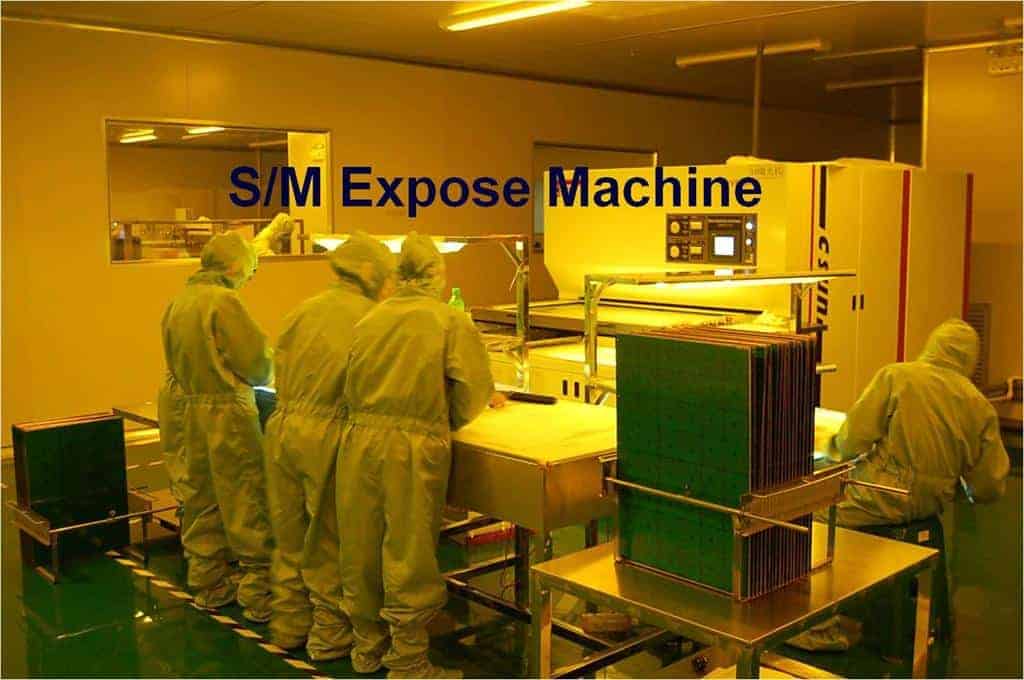
8. Photolithography
Now the panelized boards undergo photolithography which uses photo masks and chemical exposure to create required conductive pattern onto the copper layers. Key sub-steps are:
Lamination Resist – First a photosensitive epoxy dry film resist gets hot roll laminated onto boards.
Mask Imaging – The resist coating undergoes light exposure through the mask containing the desired circuit pattern image.
Developing – The resist gets developed in chemical baths revealing underlying copper at unexposed areas while retaining resin at imaged pattern.
So post lithography, the panel boards have selectively exposed copper traces and pads surrounded by epoxy resist insulation.
9. Etching
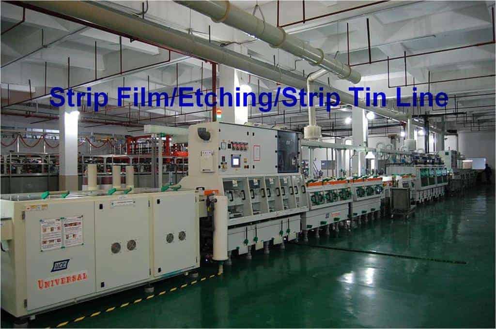
Next step removes all excess copper not protected by photoresist mask through chemical dissolution resulting in desired conductor pattern.
Etchant Selection – Common etchants like ferric chloride and ammonium persulfate dissolve copper. They work uniformly across micro-roughened high surface area foil.
Controlled Etching – Printed boards get immersed in etchant baths ensuring sufficient engraving times for complete copper clearing without excess over-etching. Over-etching undercuts traces lifting off resist. Panel agitation accelerates etch rate.
Stripping – Once etching finishes, the dry film gets stripped away revealing pristine copper circuitry ready for next fabrication stages.
10. Solder Mask Application
The exposed routed copper traces now need protective solder coating to guard against oxidation and prevent solder bridges.
Solder Resist – Flame retardant epoxy resin with green hue gets applied by curtain coating, silkscreen, electrodeposition or spray methods. The viscous resin adheres uniformly across board surface.
Photoprocessing – The solder mask resin cures partially before undergoing lithographic exposure. Photo tools selectively prevent resin curing at solder pads and connectors.
Developing – The solder mask gets developed dissolving uncured resin exposing pads and contacts. Cured mask remains over insulating zones.
Curing – Boards pass through curing oven for final solder mask hardening leaving protective layer with openings at conductive locations.
11. Silkscreen Printing
Identification printing or legend printing adds markings onto the solder masked surface to identify components, logos, board name etc.
Screen Prepare – High mesh stainless screens get designed containing text or images to be transferred.
Ink Printing – UV curable ink gets squeezed through screens onto boards by automated squeegees.
Curing – Strong UV light quickly cures and dries printed ink paste leaving durable surface markings.
Silkscreen provides product branding while assisting troubleshooting and assembly.
12. Surface Finishes
PCBs undergo metal plating of contact areas to protect exposed copper from corrosion and prepare for soldering.
OSP Coating – Organic surface protectant gets applied on fingers and pads by dipping or spraying. It serves as solderability preservative giving limited shelf life.
IMM Ag Plating – Boards undergo electrolytic deposition of silver layer in precious metal immersion (PMI) tanks before getting coated with flash gold for maximum shelf life and solderability.
ENIG Finish – Electroless nickel gold (ENIG) process deposits nickel corrosion barrier followed by an immersion gold layer for longest lasting shelf life retaining solderability. But costlier process.
HASL Finish – In Hot air solder leveling process boards pass through molten solder wave bath depositing leveled solder alloy coating on pads. Ideal for through-hole component soldering.
13. Electrical Testing
Fabricated boards undergo extensive electrical test regimen to validate conductive continuity correctness:
Flying Probe – Automatic flying probes make contact at test points across board to check for short circuits or opens.
Bed of Nails – Boards get pressed onto a bed of spring loaded pogo pin fixtures matched to board connectors for validation.
ICT Fixture – Tailor-made interconnection test fixtures allow testing connectivity between specific points.
Failed tests get debugged to pinpoint fabrication defects before rework or scrap recommendation.
14. Final Quality Inspection
Post electrical tests, finished boards undergo detailed inspection under microscopes checkingparameters like:
- Base material imperfections
- Conductor width and registration
- Hole quality
- Solder mask and legend defects
- Copper surface finish flaws
- Contamination or handling damage
This vital quality audit ensures only pristine boards ship out!
15. Panelization
Finally, thoroughly tested boards get routed back into larger panels for added mechanical stability during handling and shipping. Cut V-scores mark boundaries between adjacent boards for ease of subsequent depaneling by component assemblers.
16. Shipment
The finished boards with protective peel coats get carefully packed into ESD safe packaging before shipment to client facilities across the world.
Quality Considerations During PCB Fabrication
Implementing robust process controls is vital for fabricating reliable, high yielding boards:
Layer Registration – Tight X-Y alignment ensures no skew between layers causing routing congestion or functionality loss from net open circuits.
Impedance Control – Dielectric thickness and trace dimensions require careful modeling and measurements to achieve target impedance tolerances.
Surface Finish – Monitor surface roughness, coating thickness and solder leaching to control wetting, assembly yields and long term reliability.
CAF Resistance – Minimize conductive anodic filaments (CAF) promoting shorting risk in high humidity, voltage bias conditions.
First Pass Yields – Improving yields reduces scrap costs but needs monitoring to nip failure modes.
Once familiar with the elaborate sequence of printed circuit board fabrication steps spanning days of processing, one truly appreciates the intricate engineering culminating in mass produced boards powering myriad electronic products!
Frequently Asked Questions
Here are some common questions about the PCB fabrication process:
Q: How long does board fabrication process take?
For standard specifications, typical fabrication timeline is around 3 weeks from order placement to shipment of finished boards. But complex board construction involving harder tooling, sourcing challenges or capacity bottlenecks tends to require 4-6 week lead times.
Q: Which PCB fabrication steps impact cost the most?
High layer count builds with blind/buried vias, fine line spacings, advanced materials like ceramic or metal core substrates tend to require additional process steps or lower yields thereby increasing cost.
Q: How to assess capability of a PCB manufacturer?
One can audit their certifications like ISO, IPC Confirm uniforms process controls. Also assess range of board technologies like HDI, Rigid-flex, substrate materials handled along with engineer-to-engineer technical engagement capability.
Q: What are key considerations around PCB fabrication?
Important considerations include – electrical constraints like target impedance, high speed interfaces; mechanical requirements like board stiffness, dimensional stability, thermal dissipation needs and component assembly compatibility.
Q: How to reduce chances of fabrication defects?
Engage PCB partner early sharing your constraints. Let them review design recommendations around layer counts, stackups, breakout routing and share feedback for enhancing yield and fabrication success.
This concludes the elaborate PCB fabrication process starting from product design conception all the way to shipping reliably built boards in volume. With attention to quality processes and fabrication-friendly design, you can ensure your complex boards get manufactured right the first time itself!


0 Comments