
How can I design my own PCB?
Printed Circuit Boards (PCBs) are the backbone of modern electronics. They provide a physical platform for mounting and interconnecting electronic components, allowing complex circuits to be built in a compact and reliable manner. Designing your own PCB can be a rewarding experience, whether you’re a hobbyist, maker, or professional engineer. It gives you complete control over the layout, component selection, and overall functionality of your electronic project.
In this comprehensive guide, we’ll explore the process of designing your own PCB from start to finish. We’ll cover the essential tools, design techniques, and best practices to help you create high-quality PCBs that meet your project requirements.
Understanding PCB Design
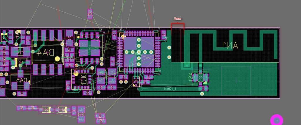
Before we dive into the design process, it’s important to understand the fundamentals of PCB design. A PCB is essentially a sandwich of conductive layers separated by insulating material. The conductive layers are etched with traces, which act as electrical pathways connecting the various components mounted on the board.
There are several key elements that make up a PCB:
- Layers: PCBs can have one or more conductive layers, depending on the complexity of the design. Single-layer PCBs are the simplest, while multi-layer PCBs offer more routing flexibility and higher component density.
- Traces: These are the conductive paths on each layer that interconnect the components. Traces must be carefully routed to avoid signal integrity issues, such as crosstalk and electromagnetic interference (EMI).
- Pads: These are the copper areas on the PCB where components are soldered or mounted.
- Vias: These are plated-through holes that allow electrical connections between different layers of the PCB.
- Silkscreen: This is the printed text and component outlines on the PCB, providing visual references for assembly and component identification.
- Solder mask: This is a protective coating applied over the copper traces to prevent solder bridges during assembly.
Understanding these elements and their relationships is crucial for creating a functional and reliable PCB design.
PCB Design Workflow
The PCB design process typically follows a structured workflow, which involves several steps. Here’s a general overview of the design flow:
- Schematic Capture: Create a schematic diagram of your circuit using a CAD (Computer-Aided Design) tool. This step involves representing the components and their interconnections in a logical manner.
- Library Management: Ensure that you have access to the necessary component footprint libraries for your design. These libraries contain the physical representations of the components used in your circuit.
- Component Placement: Arrange the components on the PCB layout, taking into account factors such as component clearances, thermal considerations, and signal integrity.
- Routing: Connect the components by drawing traces on the PCB layout, following design rules and guidelines to ensure signal integrity and manufacturability.
- Design Rule Checking (DRC): Verify that your PCB design adheres to the specified design rules, such as trace widths, clearances, and via sizes.
- Generation of Manufacturing Files: Once your design is complete and verified, generate the necessary manufacturing files (e.g., Gerber files) for PCB fabrication and assembly.
- Design Review and Verification: Thoroughly review your design, checking for errors, design rule violations, and potential issues before sending it for manufacturing.
- Fabrication and Assembly: Send your design files to a PCB manufacturer for fabrication and component assembly (if required).
While this is a general workflow, the specific steps and tools used may vary depending on the complexity of your project and the design software you’re using.
PCB Design Software
Choosing the right PCB design software is crucial for creating high-quality and efficient PCB layouts. There are several options available, ranging from free and open-source tools to professional-grade commercial software. Here are some popular PCB design software options:
| Software | Description | Price |
|---|---|---|
| KiCad | Free and open-source EDA suite with schematic capture, PCB layout, and 3D viewing capabilities. | Free |
| Eagle | Powerful PCB design software with a free version for non-commercial use. | Free (limited) / Paid |
| Altium Designer | Professional-grade PCB design software with advanced features and integrated design environment. | Paid (Subscription) |
| Cadence Allegro | High-end PCB design software used by many large electronics companies. | Paid (Subscription) |
| DesignSpark PCB | Free PCB design software from RS Components, suitable for simple to moderately complex designs. | Free |
The choice of software often depends on your budget, design requirements, and the level of complexity you’re working with. Free and open-source tools like KiCad and DesignSpark PCB can be great options for hobbyists, makers, and students, while professional engineers and companies may prefer more advanced and feature-rich commercial software like Altium Designer or Cadence Allegro.
Design Techniques and Best Practices
Creating a high-quality PCB design involves more than just connecting components with traces. There are several techniques and best practices that you should consider to ensure your design is reliable, efficient, and manufacturable.
Component Placement
Proper component placement is crucial for ensuring signal integrity, thermal management, and ease of assembly. Here are some guidelines to follow:
- Group related components together to minimize trace lengths and reduce signal noise.
- Position high-power components away from sensitive analog components to minimize electromagnetic interference (EMI) and thermal coupling.
- Place components with high pin counts (e.g., microcontrollers, FPGAs) in areas with sufficient routing space.
- Arrange components in a way that minimizes trace crossovers and reduces the risk of signal crosstalk.
- Consider the physical constraints of your enclosure or chassis when placing components.
Trace Routing
Trace routing is an essential aspect of PCB design that can significantly impact signal integrity and electromagnetic compatibility (EMC). Here are some best practices for trace routing:
- Use appropriate trace widths and clearances based on the design rules and current-carrying requirements.
- Route critical signals (e.g., clocks, high-speed data) with controlled impedance and minimize stubs and vias.
- Use ground planes and power planes to provide low-impedance return paths and minimize EMI.
- Avoid sharp 90-degree turns in traces, as they can introduce signal reflections and ringing.
- Minimize trace lengths for high-speed signals to reduce propagation delays and signal degradation.
- Use serpentine or meandering traces to match the length of differential pairs or timing-critical signals.
- Separate sensitive analog signals from high-speed digital signals to minimize crosstalk and interference.
Power and Ground Distribution
Proper power and ground distribution is essential for ensuring stable and reliable operation of your electronic circuits. Here are some best practices:
- Use dedicated power and ground planes (or polygons) for low impedance and efficient power distribution.
- Provide adequate decoupling capacitors near power pins of integrated circuits to suppress high-frequency noise.
- Separate analog and digital ground planes (or polygons) to minimize noise coupling.
- Use star ground topology for sensitive analog circuits to prevent ground loops.
- Implement proper filtering and bypassing techniques for power supply inputs and outputs.
Design for Manufacturing (DFM)
When designing your PCB, it’s important to consider the manufacturability of your design. Here are some DFM guidelines:
- Follow the PCB manufacturer’s design rules and specifications for trace widths, clearances, and via sizes.
- Avoid acute angles and sharp corners in your traces, as they can be difficult to etch accurately.
- Ensure adequate clearance around mounting holes and board edges.
- Provide sufficient space for component placement and assembly operations.
- Consider using standard component footprints and packages whenever possible.
- Implement design features (e.g., fiducials, alignment marks) to aid in automated assembly processes.
Design for Testability
Designing for testability ensures that your PCB can be easily tested and debugged during the prototyping and manufacturing stages. Here are some best practices:
- Include test points or probing pads for critical signals and power/ground connections.
- Provide access to programming and debugging interfaces (e.g., JTAG, SWD) if your design includes programmable devices.
- Consider adding boundary scan (JTAG) support for complex designs with multiple programmable devices.
- Implement design partitioning and modular approaches to simplify testing and debugging.
Signal Integrity
Signal integrity is critical for ensuring reliable and error-free operation of high-speed digital circuits and analog circuits with sensitive signals. Here are some techniques to improve signal integrity:
- Use controlled impedance routing for high-speed signals (e.g., differential pairs, clock signals).
- Implement proper termination and matching for high-speed signals to minimize reflections and ringing.
- Use signal shielding techniques (e.g., ground planes, guard rings) to minimize crosstalk and EMI.
- Implement proper decoupling and bypassing techniques to suppress power supply noise.
- Minimize trace lengths and vias for critical signals to reduce propagation delays and signal degradation.
Thermal Management
Proper thermal management is essential for ensuring the reliable operation and longevity of your electronic devices. Here are some best practices:
- Place high-power components (e.g., power regulators, processors) in areas with good airflow and thermal dissipation.
- Use thermal vias and thermal reliefs to improve heat transfer from power components to the PCB.
- Consider adding heat sinks or dedicated thermal planes for high-power components.
- Implement proper spacing and clearances around hot components to prevent heat buildup and thermal coupling.
- Consider thermal simulation and analysis for complex designs with high power dissipation.
Design Documentation
Documenting your PCB design is crucial for maintaining design integrity, facilitating future modifications, and enabling collaboration with others. Here are some best practices for design documentation:
- Create detailed schematics and block diagrams that clearly represent the functionality and interconnections of your design.
- Maintain a comprehensive bill of materials (BOM) that lists all components, their specifications, and quantities.
- Document design rules, constraints, and any specialized design techniques used.
- Include clear and concise notes, labels, and annotations on your PCB layout to aid in assembly and troubleshooting.
- Create a design review report that documents any design decisions, trade-offs, and potential issues.
- Maintain version control and revision history for your design files.
Following these design techniques and best practices will help you create high-quality, reliable, and manufacturable PCB designs that meet your project requirements.
Frequently Asked Questions (FAQs)
- What is the minimum number of layers required for a PCB design? The minimum number of layers for a PCB design is one, which is known as a single-layer PCB. However, for more complex designs with high component density or signal routing requirements, multi-layer PCBs (e.g., 2-layer, 4-layer, or more) are often necessary.
- Can I design a PCB without using CAD software? While it is technically possible to design a PCB manually using traditional drafting techniques, it is not recommended due to the complexity and precision required for modern PCB designs. CAD software is essential for efficient and accurate PCB design, and it also provides tools for design rule checking, component management, and manufacturing file generation.
- How do I choose the right PCB design software? The choice of PCB design software depends on several factors, including your budget, design requirements, and the level of complexity you’re working with. Free and open-source tools like KiCad and DesignSpark PCB can be great options for hobbyists, makers, and students, while professional engineers and companies may prefer more advanced and feature-rich commercial software like Altium Designer or Cadence Allegro.
- What file formats are used for PCB manufacturing? The most common file formats used for PCB manufacturing are Gerber files and Excellon drill files. Gerber files contain the copper layer patterns, solder mask, silkscreen, and other essential information for the PCB fabrication process. Excellon drill files specify the locations and sizes of the drill holes for components and vias.
- How can I ensure my PCB design is manufacturable? To ensure your PCB design is manufacturable, follow the design rules and specifications provided by the PCB manufacturer. This includes adhering to trace width and clearance requirements, via size constraints, and any other guidelines specific to the manufacturing process. Additionally, implement design for manufacturing (DFM) best practices, such as avoiding acute angles and sharp corners in traces, providing adequate clearances, and using standard component footprints whenever possible.
Conclusion
Designing your own PCB can be a rewarding and empowering experience, whether you’re a hobbyist, maker, or professional engineer. By following the techniques and best practices outlined in this guide, you can create high-quality, reliable, and manufacturable PCB designs that meet your project requirements.
Remember, PCB design is an iterative process that often involves trial and error, design revisions, and continuous learning. Don’t be discouraged by setbacks or challenges; instead, embrace them as opportunities to improve your skills and gain valuable experience.
With the right tools, knowledge, and persistence, you can bring your electronic designs to life and unlock a world of possibilities for your projects.