Introduction
Printed circuit boards (PCBs) are essential components in almost all modern electronic devices. They provide the foundation on which components like integrated circuits, resistors, capacitors and LEDs are mounted and interconnected. As LEDs become increasingly popular for lighting applications due to their energy efficiency, brightness and long lifespan, understanding the manufacturing process for LED PCB assemblies is crucial for producing high quality and reliable products. This article provides a comprehensive overview of the key steps and considerations involved in LED PCB assembly.
PCB Design and Layout
The first step in creating an LED PCB assembly is designing and laying out the printed circuit board itself. Some key factors to consider during PCB design include:
Component Placement
Carefully place components according to LED layout requirements, proximity to heat sources, and ease of manufacturing. Group related components together when possible.
Thermal Management
Incorporate design elements like thermal pads and vias to facilitate heat dissipation from high-power LEDs. This helps prevent overheating and extends LED lifespan.
Board Size and Shape
Consider the end product requirements and enclosure constraints when designing PCB dimensions. Allow room for connectors, mounting holes, and other required hardware.
Copper Thickness
Use thicker copper layers for power and ground planes to handle the current demands of multiple LEDs. Thinner copper for other traces to optimize cost and weight.
Solder Mask and Silkscreen
Design solder mask and silkscreen layers to prevent solder bridging and clearly identify component locations, orientations, and values.
Sourcing LED Components
Once the PCB design is finalized, the next key step is sourcing the required LED components:
LED Packages
Select LED packages (SMD, COB, etc) appropriate for the lighting application and arrange them on the PCB according to design requirements. Match electrical parameters like drive current, voltage, and thermal characteristics.
LED Drivers/Controllers
Choose compatible LED driver ICs or discrete circuits to provide the correct current and voltage to each LED string. Consider factors like dimming capability, efficiency, and form factor.
Passive Components
Source accompanying passive components like resistors and capacitors to complement the LED driver circuits and other functional blocks.
Connectors
Obtain suitable connectors for interfacing the LED PCB with external circuits, power supplies, and controls. Common connectors used include screw terminals, molex connectors, and JST connectors.
Thermal Interface Materials
For high-power LED assemblies, thermal interface materials like thermal pads or heat sinks will be needed to maximize heat transfer away from the LEDs during operation.
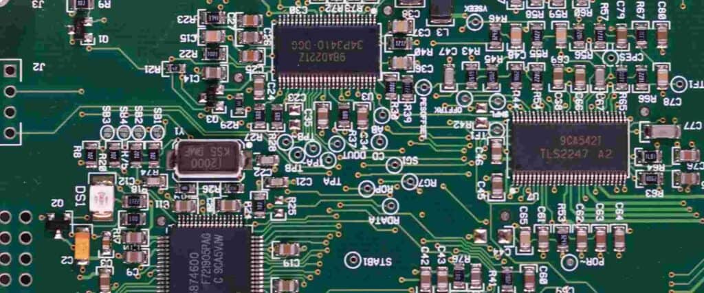
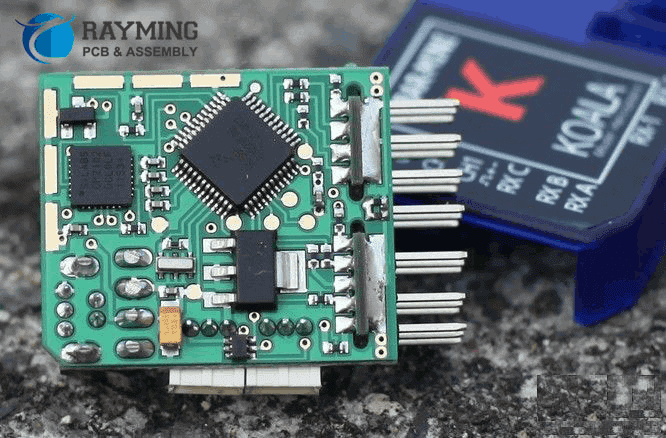
SMT Assembly Process
With all the components sourced, the next stage is SMT (surface mount technology) assembly of the PCB. Here are some key steps:
Solder Paste Application
Solder paste containing tiny lead-free solder alloy particles mixed with flux is first applied on PCB pads using stencil printing.
Component Placement
SMT pick-and-place machines then assemble the PCB by rapidly picking components from reels or trays and accurately placing them on their designated pads.
Solder Reflow
The PCB enters a reflow oven where the temperature profile melts the solder paste causing components to be permanently soldered in place.
Inspection and Testing
Automated optical inspection and electrical testing checks for defects and verifies assembly quality before boards proceed further.
Conformal Coating
For boards in challenging environments, a protective conformal coating may be applied to guard against moisture, contaminants, and corrosion.
##Through-Hole Assembly
In addition to SMT components, many LED PCBs also utilize through-hole parts which require insertion and soldering of wire leads or pins. Common steps include:
Component Insertion
Larger through-hole LEDs, wiring connectors, and other parts are inserted into their designated PCB holes either manually or via automatic insertion machines.
Wave Soldering
The assembled PCB passes over a wave of molten solder, soldering inserted component leads/pins in one process.
Selective Soldering
Supplementary soldering is done via selective soldering machines to fill any missing joints post wave soldering.
Additional Soldering
Certain connectors, wires, or components may require hand soldering afterwards to complete assembly.
Programming and Functionality Testing
Once fully assembled, the LED PCB must be programmed and have its functionality validated.
Microcontroller Programming
For PCBs with microcontrollers, appropriate firmware/software is loaded to dictate LED behavior. Done via programming interfaces like JTAG, ISP, SWD, etc.
LED Mapping
LED strings may be mapped/addressed to activate the correct groups together and perform dynamic lighting effects.
Power-On Testing
Basic power-on testing validates that LEDs turn on and driver circuits perform properly. Input/output signal checking also done.
Functional Testing
Boards are put through simulation of actual end-use conditions across temperature, humidity, electrical noise, etc to verify robust operation.
Quality Assurance
Throughout the assembly process, rigorous quality control steps ensure consistently high production standards:
Incoming Component Inspection
All incoming components are inspected for authenticity, correct specifications, and absence of damage before being committed to production.
Process Control Monitoring
Critical assembly process parameters like soldering temperature profiles, pick-and-place precision, etc are closely monitored.
Statistical Process Control (SPC)
Key metrics are tracked using control charts to detect process deviations and implement improvements before defective product is made.
Automated Optical Inspection (AOI)
AOI systems quickly scan assembled PCBs and compare with computer models to identify component defects.
Environmental Stress Testing
Samples boards undergo testing under extreme conditions (temperature cycling, vibration, etc) to confirm the assembly can withstand end-use environments.
Summary
In summary, modern LED PCB assembly is a complex, multi-stage manufacturing process requiring careful design, component selection, assembly optimization, testing, and quality control to produce a fully functional lighting product. The guidelines presented in this article provide a high-level overview of key considerations across the end-to-end production cycle for creating reliable and high-performing LED assemblies.
FAQ
Q: What are some common PCB substrates used for LED assemblies?
A: The most common PCB substrates are FR-4 (glass reinforced epoxy), aluminum, and ceramic. FR-4 provides good electrical insulation at low cost. Aluminum and ceramic offer superior thermal conductivity to dissipate heat.
Q: What solder alloys are used to assemble LED PCBs?
A: SAC alloys (tin/silver/copper) are the predominant Pb-free solder choice for LED PCB assembly due to their reliability, wettability, and performance at high temperatures. SAC305 (3% silver, 0.5% copper) is a popular and widely used variant.
Q: How is inspection done to check for soldering defects?
A: Automated optical inspection (AOI) is commonly used to check solder joints on assembled PCBs. Other techniques include X-ray inspection and automated X-ray inspection (AXI) which can detect hidden defects like voids or insufficient solder.
Q: What are some best practices to manage heat on high power LED PCBs?
A: Using metal core PCBs, thermal vias, solder pads, and heat sinks help conduct heat away from LEDs. Careful component placement also avoids concentrated heat pockets. Managing drive current and pulse modulation helps reduce heating effects.
Q: How are LEDs typically protected from electrical spikes or transients?
A: On-board transient voltage suppressors (TVS diodes), surge protection devices, and other voltage clamping components protect LEDs. Fuses, current limiting resistors, and robust driver circuits also improve electrical robustness.


0 Comments