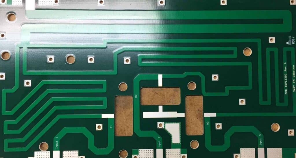
Printed circuit boards (PCBs) are used to mechanically support and electronically connect electronic components using conductive pathways or traces etched from copper sheets laminated onto a non-conductive substrate. When high frequency signals are transmitted through these traces, the impedance needs to be controlled to prevent issues like reflections or electromagnetic interference (EMI).
Impedance is a measure of opposition to alternating current (AC). For PCBs, it applies to the conductive trace’s ability to resist high frequency AC signals. Impedances can be designed for signal matched conditions to eliminate reflections. Understanding PCB stackup configurations and trace geometry is key to tuning trace impedances.
This article will cover methods for calculating a PCB trace’s impedance based on its physical dimensions and layout materials. We’ll explore the importance of controlled impedance traces, equations to model impedance, stackup parameters, and tips for impedance calculators.
Why Control Impedance?
For low speed or direct current (DC) applications, PCB traces can simply be designed to conduct enough current. But with today’s high speed digital signals, uncontrolled impedances lead to reflections and EMI that corrupt signal integrity.
Controlling trace impedances to match transmitter, receiver, and cable impedances eliminates reflections and smooths transmission across the system. This is done through careful PCB stackup design and trace dimensioning relative to reference planes. If the source, transmission lines, and load are mismatched, parasitic capacitance and inductive impedance effects occur.
By mathematically modeling the trace geometry and materials as an electrical transmission line, we can tune the traces for target impedance characteristics. Precision impedance traces ensure proper function of frequency dependent components.
Equations for Modeling PCB Impedance
There are mathematical equations that model a PCB trace over a reference plane as an electrical transmission line with parasitic resistance, inductance, capacitance, and conductance. The impedance can be tuned by adjusting physical parameters like trace width/thickness, spacing to planes, or dielectric materials.
Single-Ended Impedance
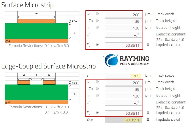
For a single trace routed over a reference plane without an adjacent ground plane, the impedance can be calculated with the Stripline Impedance Equation:Copy code
Z0 = (87 / √εr) * ln[(5.98*h) / (0.8*w + t)] Where: Z0 = Impedance (ohms) εr = Dielectric constant of laminate material h = Trace height above reference plane (mils) w = Trace width (mils) t = Trace thickness (mils)
This simplified equation models the trace as an electrical transmission line to solve for impedance, which helps match connected components. Reference plane distance and trace dimensions are the key physical parameters.
Differential Pair Impedance
For differential pair routing with adjacent traces over a ground plane, the Differential Impedance Equation is used:Copy code
Zdiff = (138 / √εr) * ln[(4*h) / (0.67π * (0.8*w + t))] Where: Zdiff = Differential impedance (ohms) εr = Dielectric constant h = Trace height above plane (mils) w = Trace width (mils) t = Trace thickness (mils)
This adds the gap width between traces as a factor for impedance. Tuning trace gaps and widths together is key for differential signals.
PCB Stackup Configuration Parameters
To accurately determine impedance, we must understand the PCB layer stackup:Copy code
| Layer | Function | |----------|--------------------------------| | Layer 1 | Component side copper | | Layer 2 | Ground reference plane | | Layer 3 | Dielectric core laminate | | Layer 4 | Power reference plane | | Layer 5 | Dielectric core laminate | | Layer 6 | Solder side copper layer |
Relevant parameters include:
- Dielectric Constant (Dk / εr) – Material property affecting propagation velocity
- Copper Weight – Thickness of copper foil (1oz = 1.4 mils thickness)
- Trace Width – Width of routed trace
- Trace Height – Distance between trace center to reference plane
- Glass Weave % – Amount of glass fibers affecting Dk
These physical factors all influence impedance for more accurate modeling. Identifying parameters from your PCB stackup is required before calculating impedances.
Tips for Using Impedance Calculators
Most PCB layout software packages include impedance calculators. They apply the transmission line equations, taking inputs for the stackup parameters and trace dimensions. This allows interactive tweaking of values to target specific impedance needs.
Here are some tips for working with impedance calculators:
- Confirm stackup details like layer thickness, materials, copper weight
- Enter dielectric constants correctly for materials
- Set trace width constraints based on current needs
- Enter multiple trace height values to plot impedance vs height
- Account for glass weave (e.g. reduce εr by ~20%)
- Target 50 Ohm or 75 Ohm differential impedance
- Ensure impedance tolerance sufficient for application
- Save common configurations as impedance profiles for reuse
With the right inputs, calculators allow modeling of how proposed geometries affect impedance before routing begins. Different stackups and line widths can be simulated to guide initial layout.
Reviewing impedance graphs also helps visualize the impact of variables. This helps narrow the acceptable trace dimensions and stackup configurations for a target application.
Differential Pair Routing Guidelines
To achieve balanced differential impedances for twin traces, follow these guidelines:
- Match electrical lengths to ensure consistent propagation delays
- Use symmetric trace widths for uniform line resistance
- Eliminate length differences beyond 1/10 signal wavelength
- Capacitive imbalance under 5%
- Route pairs on outer layers for design control
- Minimize number of vias, with careful length matching
- Remove unused traces between pairs
- Avoid 90° turns to reduce skew risk
Tuning the spacing between traces is key – slight gaps changes cause substantial impedance deviations. But moving in sync, a balanced impedance differential pair can effectively carry very high frequency signals across the PCB with minimal distortion.
Sample Differential Routing Stackup
Here is an example 4-layer PCB stackup for a 100 Ohm differential pair over 50 Ohms to ground, with target parameters:Copy code
| Layer | Description | |----------|------------------------------------------| | Layer 1 | Signal traces (5 mil thickness) | | Layer 2 | Ground plane (1 oz) | | Layer 3 | Core dielectric (4 mils thick, εr=4.5) | | Layer 4 | Power plane (1 oz) | Trace Width: 6 mils Trace Gap: 6 mils Routing Height: 4 mils (center-to-plane)
Plugging this into our differential impedance equation, the traces model closely to our 100 Ohm differential target. Small adjustments to the gap or widths can fine tune as needed.
Comparisons of Calculator Methods
There are a few analysis methods used by impedance calculators to model effects of trace geometry on impedance:Copy code
| Method | Description | Accuracy | |---------------------|------------------------------------------------------|----------| | 2D Cross-Section | Simplified model good for initial estimates | Fair | | Planar E.M. | Models copper thickness impact | Good | | Multi-layer E.M. | Accounts for additional layers in stackup | Better | | 3D E.M. Simulation | Models complex field interactions in three planes | Best |
More advanced numerical solving of Maxwell’s equations in the material can provide greater modeling fidelity – at the cost of simulation compute time. The optimal method depends on the acceptable tolerance to balance precision and design time.
Setting Target Impedance Values
Default target impedance values are set based on common standards:
- Single-ended – 50, 75 or 100 Ohms
- Differential – 100 Ohm differential / 50 Ohm to ground
But the optimal impedance targets vary by application based on factors like:
- Signal frequencies used
- IC driver characteristics
- Line length matching needs
- Layer stackup materials and costs
Wider values are sometimes used – like 85 or 130 Ohm differential pairs over 75 Ohm single-ended references. Simulating and comparing candidate values helps guide ideal targets.
Controlled impedance lines only work when the source, transmission trace, and load are matched. So the driving and receiving elements must also be specified for the same target impedance levels. Termination schemes are often used to match interconnects.
High Speed Layout Guidelines
For multi-gigabit PCB designs, tightly control both impedance AND time delay to ensure signal integrity:Copy code
| Parameter | Goal | | -------------------- | --------------------------------------------------| | Impedance | Match components and transmission lines | | Propagation Delay | Match delay between signals | | Cross-talk | Eliminate coupling on parallel traces | | Reflection Noise | Terminate traces to minimize reflections | | Phase Delay Skew | Minimize skew between differential pairs | | Loss Per Unit Length | Low enough for signal power level at receiver |
This requires careful routing practices:
- Reference planes close to signals
- Short direct trace paths
- Avoid stubs or branches
- Symmetric routing patterns
- Components placed for timing
With controlled impedance transmission lines, multi-gigabit data rates can be achieved as signals transmit rapidly across a PCB with minimal interference.
Effects of PCB Materials on Impedance
The dielectric constant (Dk / εr) influences impedance calculations as it impacts propagation velocity in the material. Some guidelines on materials:
- FR-4 Glass Epoxy – Most common, low cost, εr ~4.5
- High εr (ferrite) – Slows edge rates for reflections
- Low Dk laminates – Increases velocity, improves impedance uniformity
- Low loss laminates – Reduces signal loss per inch
Also consider consistency – glass weave causes localized Dk variations that affect impedance precision. Model differences in glass percentage to improve accuracy.
Advanced PCB materials continue to emerge, allowing designers to tailor electrical performance. This expands options for dialing in target impedance characteristics.
Effects of Construction on Impedance
Fabrication factors that alter trace geometry will skew impedance away from modeled values:Copy code
| Construction Issue | Effect on Impedance | |------------------------|--------------------------| | Trace width tolerance | Shifts by +/- few ohms | | No reference planes | Severe impedance spikes | | Faulty lamination | Voids change Dk | | Routing irregularities | Reflections introduced | | Poor plane bonds | RF return path loss | | Overetched traces | Alters transmission line |
Careful stackup design, layout practices, and manufacturing checks help maximize impedance control. But even minor factors can cumulatively alter target values and signal performance.
verification and testing methods
To validate impedances match calculated models, a few measurement and simulation techniques help characterize fabricated boards:
- TDR Testing – Time domain reflectometry compares impedance over line length
- VNA Measurements – Swept frequency methods sense discontinuities
- Signal Integrity Simulations – Model wave propagation to catch distortions
- Eye Diagram Analysis – Evaluate signal fidelity with live data signals
This quantifies variations from target impedance levels and the resulting effects on signal quality – whether due to construction defects or the inherent limitations of theoretical modeling. Adjustments can then refine impedance accuracy.
Carefully correlating measured results with calculated models tunes the precision of PCB impedance. This builds data for better modeling parameters and design rules to support reliable applications.
Why Controlled Impedance Traces are Essential for Signal Integrity
As operational frequencies push into the multi-gigahertz range, controlled impedances are a necessity for clean signal transmission. Uncontrolled traces will severely distort signals beyond just hundreds of megahertz.
But a properly designed impedance matched network, aligned to your signal specifications and PCB stackup, will maintain superior signal integrity even near 10 GHz. This allows high speed components to perform reliably at their rated levels.
Pros and Cons of Various Impedance Modeling Methods
There are always tradeoffs when selecting an analysis method to calculate target PCB impedance levels:Copy code
| Method | Pros | Cons | |--------------------------------------- | ---------------------------------|-------------------------------------------- | | Analytic Equations | Simple, fast | Limited accuracy | | 2D Cross-section Calculator | Good visualization | Assumes TEM mode fields | | Planar EM Solver | Models thickness, runtime fast | Requires meshing | | 3D EM Simulation | Highest accuracy | Complex models, extensive compute time | | Spreadsheet Calculator | Free, editable | Risk of errors | | Integrated Layout Tool | Links routing, DRC | Cost, software learning curve |
Determine analysis fidelity needed, then leverage the optimal toolset to sufficiently characterize traces while meeting project schedule needs.
Conclusion
With today’s multi-gigabit digital systems, controlled impedance PCB traces are essential to maintain signal integrity under high frequencies. This eases routing while ensuring matched transmission lines between components that eliminate reflections while preventing EMI.
By modeling traces as electrical transmission lines, mathematical equations help target impedance based on physical construction parameters. Values are tuned through trace dimensions and widths, along with dielectric constants and distances to reference planes.
Reviewing impedance simulations while adjusting line geometries and board materials helps dial in characteristics. Advanced modeling and simulations also improve calculation precision. Construction care further safeguards performance.
With the right modeling methodology selected, target impedances defined, routing practices that maximize SI, and manufacturing vigilance – multi-gigabit signals will transfer swiftly across a PCB with minimal interference or losses. Careful impedance control ensures clean high speed operation.
Frequently Asked Questions
Below are answers to common questions related to calculating the impedance of PCB traces:
1. Does every PCB trace need controlled impedance?
No, controlled impedance traces are only required for high frequency signals generally over 50 MHz. Lower frequency digital signals or DC power nets do not need impedance control.
2. How accurate do my models need to be for calculating impedances?
Tolerance requirements depend on the signals. For example, ±10% is generally sufficient for impedance control, while matched delay requires tighter ±5% correlation between modeled and measured results.
3. My 100 Ohm differential pair is showing simulated impedance around 85 Ohms – what’s wrong?
Check if the stackup materials properties are properly specified, including dielectric constants and glass weave amounts which directly influence impedance accuracy. Construction variations could also alter values.
4. I adjusted a trace neckdown region – will this cause impedance discontinuities?
Potentially yes, as any abrupt structural change like width adjustments or stubs will introduce impedance discontinuities and reflections. Replace neckdowns with tapers to gradually change dimensions over longer lengths.
5. What test equipment can I use to measure impedances of traces?
Time domain reflectometry (TDR) systems allow measuring a trace’s impedance profile while vector network analyzers (VNAs) characterize impedance variations with frequency. This quantifies deviations from target values.


0 Comments