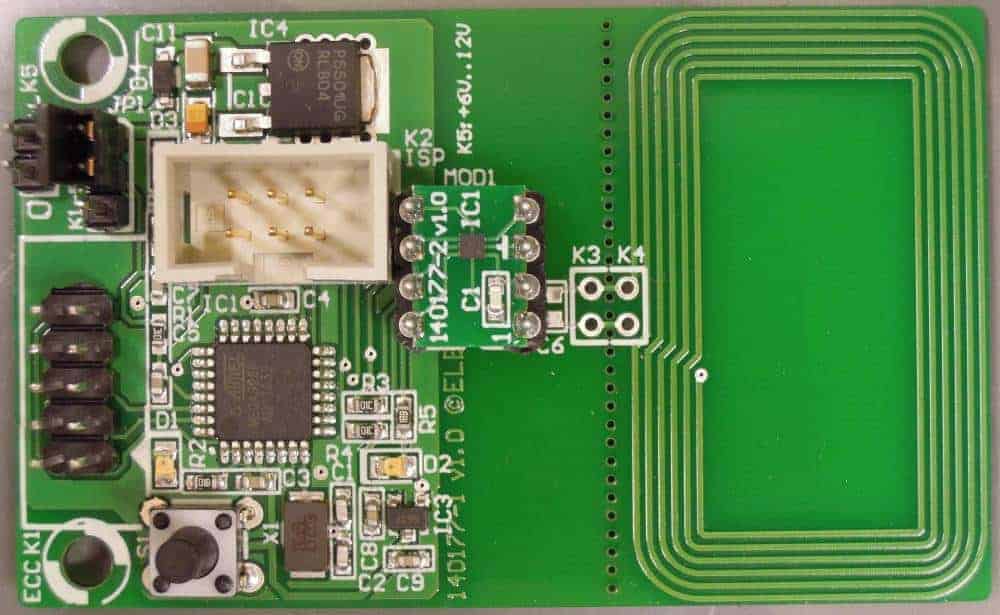
In the realm of electronics, the printed circuit board (PCB) is a crucial component that forms the backbone of most electronic devices. It serves as a foundation for mounting and interconnecting various electronic components, enabling the seamless flow of electrical signals. One of the key elements of a PCB is the trace, which plays a vital role in establishing these interconnections.
Traces are the conductive pathways etched onto the PCB’s surface or embedded within its layers. They act as tiny wires, allowing electrical signals to travel from one point to another, facilitating communication between the various components mounted on the board. Without these intricate traces, electronic circuits would be virtually impossible to construct and function properly.
In this comprehensive article, we will delve into the world of PCB traces, exploring their types, materials, design considerations, and their significance in the overall performance and reliability of electronic devices.
Types of Traces
PCB traces can be classified into several categories based on their physical location and construction within the board. The primary types of traces include:
1. Surface Traces
Surface traces are the most common and visible type of traces found on PCBs. They are etched onto the outer layers of the board, typically made of copper. These traces are exposed and can be easily seen with the naked eye.
2. Buried Traces
Buried traces, as the name suggests, are embedded within the internal layers of a multi-layered PCB. They are sandwiched between the board’s insulating layers and are not visible from the outside. Buried traces are often used to optimize signal routing and reduce electromagnetic interference (EMI).
3. Blind Vias
Blind vias are conductive pathways that connect traces on different layers but do not extend through the entire thickness of the PCB. They are commonly used to facilitate signal transitions between layers without the need for through-hole vias, which can consume valuable board space.
4. Micro Traces
Micro traces are extremely thin and densely packed conductive pathways used in high-density interconnect (HDI) PCBs. These traces are typically smaller than the standard trace widths, allowing for more compact and intricate designs, especially in applications where space is at a premium, such as smartphones and wearable devices.
Trace Materials
The most commonly used material for PCB traces is copper, owing to its excellent electrical conductivity and affordability. However, in specialized applications or for specific performance requirements, other materials may be employed:
- Copper: Copper is the industry-standard material for PCB traces due to its high electrical conductivity, durability, and cost-effectiveness.
- Aluminum: Aluminum traces are sometimes used in applications where weight is a critical factor, as aluminum is lighter than copper. However, aluminum has a lower electrical conductivity compared to copper.
- Gold: Gold traces are employed in high-frequency applications and in environments where corrosion resistance is crucial. Gold has excellent electrical conductivity and does not oxidize, making it suitable for applications requiring long-term reliability.
- Silver: Silver is another highly conductive material used for traces, particularly in radio-frequency (RF) and microwave applications. It offers superior electrical performance compared to copper but is more expensive and prone to migration issues.
- Alloys: Various alloys, such as copper-nickel or copper-tin, can be used for traces in specialized applications where specific properties, such as resistance to corrosion or electromigration, are required.
Trace Design Considerations
The design of PCB traces is a critical aspect that can significantly impact the performance, reliability, and overall functionality of electronic devices. Several factors must be considered when designing traces:
1. Trace Width
The width of a trace is determined by the amount of current it needs to carry and the desired resistance. Wider traces have lower resistance and can handle higher currents, but they also consume more board space. Conversely, narrower traces are more space-efficient but may have higher resistance and limited current-carrying capacity.
2. Trace Thickness
The thickness of a trace, also known as its height or plating thickness, affects its resistance and current-carrying capability. Thicker traces have lower resistance and can handle higher currents, but they also increase the overall cost and weight of the PCB.
3. Trace Spacing
The spacing between adjacent traces is crucial to prevent short circuits and ensure signal integrity. Adequate spacing is necessary to prevent electromagnetic interference (EMI) and crosstalk between signals. The spacing requirements are typically specified by industry standards or design guidelines based on the operating frequency and voltage levels.
4. Trace Routing
The routing of traces on a PCB is a complex task that involves minimizing signal path lengths, avoiding sharp corners, and ensuring proper grounding and shielding. Careful trace routing can reduce electromagnetic interference, improve signal integrity, and optimize the overall performance of the electronic device.
5. Thermal Considerations
In applications involving high currents or power dissipation, thermal management becomes a critical factor in trace design. Traces may need to be wider or incorporate additional cooling measures, such as thermal vias or heat sinks, to ensure proper heat dissipation and prevent overheating.
6. Signal Integrity
For high-speed or high-frequency applications, signal integrity is a paramount concern. Trace design must consider factors such as impedance matching, crosstalk, and reflections to ensure accurate signal transmission and minimize signal degradation.
7. Design Rules and Standards
PCB design rules and industry standards, such as IPC (Association Connecting Electronics Industries) guidelines, provide specifications and recommendations for trace design. These rules ensure compliance with manufacturing capabilities, reliability requirements, and industry best practices.
Trace Manufacturing
The manufacturing process for PCB traces involves several steps:
- Lamination: The base material for the PCB, typically a fiberglass-reinforced epoxy resin, is laminated with a conductive layer, usually copper foil.
- Photolithography: A photosensitive material (photoresist) is applied to the copper layer, and a photomask containing the trace pattern is used to selectively expose and develop the photoresist.
- Etching: The exposed areas of the copper layer are etched away, leaving behind the desired trace pattern.
- Plating: Additional layers of conductive materials, such as tin, gold, or nickel, may be plated onto the traces to enhance their properties, such as corrosion resistance or solderability.
- Drilling: Holes are drilled into the PCB for component mounting and through-hole vias, which provide electrical connections between different layers.
- Solder Masking: A solder mask, a non-conductive protective coating, is applied to the PCB surface, leaving the trace pads and component areas exposed for soldering.
- Surface Finishing: Final surface treatments, such as hot air solder leveling (HASL) or immersion silver, may be applied to improve the solderability of the traces and pads.
Trace Reliability and Testing
The reliability of PCB traces is crucial for ensuring the proper functioning and longevity of electronic devices. Several factors can impact trace reliability, including:
- Electromigration: This phenomenon occurs when high current densities cause the gradual movement of metal atoms in the trace, potentially leading to open circuits or shorts.
- Thermal Cycling: Repeated temperature fluctuations can cause mechanical stresses and fatigue in the traces, potentially leading to cracking or delamination.
- Environmental Factors: Exposure to moisture, corrosive gases, or contaminants can degrade the quality and performance of traces over time.
To ensure trace reliability, various testing methods are employed:
- Electrical Testing: Continuity and resistance measurements are performed to verify the integrity of traces and detect any open circuits or shorts.
- Environmental Testing: PCBs are subjected to accelerated environmental conditions, such as temperature cycling, humidity, and vibration, to assess their performance and durability.
- Signal Integrity Testing: For high-speed or high-frequency applications, signal integrity tests are conducted to evaluate the performance of traces in terms of impedance matching, crosstalk, and signal quality.
- Visual Inspection: Microscopic visual inspections are performed to detect any defects, such as cracks, voids, or delamination, in the traces or surrounding areas.
- Failure Analysis: In the event of trace failures, advanced techniques like cross-sectioning, scanning electron microscopy (SEM), and energy-dispersive X-ray spectroscopy (EDS) are used to identify the root cause and facilitate corrective actions.
FAQs (Frequently Asked Questions)
- What is the difference between a trace and a via? A trace is a conductive pathway on the surface or within the layers of a PCB, while a via is a plated hole that provides electrical connections between different layers of the board.
- What factors determine the maximum length of a trace? The maximum length of a trace is primarily determined by signal integrity considerations, such as impedance matching, signal attenuation, and reflections. Longer traces are more susceptible to signal degradation, especially at high frequencies.
- Can traces be repaired or modified after PCB manufacturing? Minor trace repairs or modifications are possible through techniques like jumper wires or conductive epoxy. However, major trace alterations or rerouting may require redesigning and remanufacturing the PCB.
- What is the impact of trace width on signal integrity? Trace width can affect signal integrity by influencing the characteristic impedance of the trace. Wider traces tend to have lower impedance, while narrower traces have higher impedance. Impedance mismatches can lead to signal reflections and distortions.
- How does the PCB material affect trace performance? The dielectric material used in the PCB can impact trace performance in terms of signal propagation speed, loss characteristics, and impedance control. Materials with lower dielectric constants and lower dissipation factors generally provide better high-frequency performance.
Conclusion
Traces are the lifeblood of printed circuit boards, enabling the seamless flow of electrical signals and interconnecting various components. Understanding the types, materials, design considerations, and manufacturing processes of traces is crucial for ensuring the optimal performance, reliability, and longevity of electronic devices.
From surface traces to buried traces and micro traces, each type serves a specific purpose and caters to different application requirements. Careful trace design, considering factors such as width, thickness, spacing, and routing, is essential for maintaining signal integrity, thermal management, and electromagnetic compatibility.
With the ever-increasing demand for miniaturization, high-speed signaling, and complex functionality, the role of traces in PCB design becomes even more pivotal. Advances in materials, manufacturing techniques, and design tools continue to push the boundaries of trace performance, enabling the development of cutting-edge electronic products.
As the electronics industry evolves, the importance of trace design and reliability will only continue to grow, driving the need for further research, innovation, and adherence to industry standards and best practices.


0 Comments