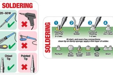
Prototype PCB Assembly
  • Home
  • SMT Assembly
  • PCB Manufacturing
  • Blog
  • Contact
  • More

Prototype PCB Assembly

PCBA

How to Remove Soldermask from Printed Circuit Boards?

What is PCB Soldermask and Why Remove It? Soldermask, also known as solder resist or solder stop mask, is a thin lacquer-like layer of polymer applied to the copper traces of a printed circuit board (PCB). Its primary purpose is to prevent solder from bridging between conductors and creating short Read more…

By Prototype PCB Assembly, 1 year ago
PCBA

The Most Common Used LPI Soldermask Application Method C Silk Screen Printing

What is LPI Soldermask? LPI (Liquid Photo Imageable) soldermask is a type of protective coating applied to printed circuit boards (PCBs) to protect the copper traces from oxidation, prevent solder bridges, and provide electrical insulation. It is a photosensitive polymer that is applied as a liquid and then cured using Read more…

By Prototype PCB Assembly, 1 year ago
PCBA

Why is Green Soldermask Most Commonly Used for PCB Fabrication?

Introduction to PCB Soldermask Printed Circuit Boards (PCBs) are essential components in modern electronics, forming the backbone of countless devices we use every day. One crucial aspect of PCB manufacturing is the application of soldermask, a protective layer that covers the copper traces on the board. While soldermask comes in Read more…

By Prototype PCB Assembly, 1 year ago
PCBA

7 Problems in the Multilayer PCB Fabrication Process

Introduction to PCB Fabrication and Common Issues Printed Circuit Board (PCB) fabrication is a complex process that involves multiple steps and requires precise control over various factors. Multilayer PCBs, in particular, pose additional challenges due to their intricate structure and the need for precise alignment between layers. In this article, Read more…

By Prototype PCB Assembly, 1 year ago
PCBA

4 Main Types of PCB Solder Mask

What is PCB Solder Mask? PCB solder mask, also known as solder resist or solder stop mask, is a thin layer of polymer applied to the copper traces of a printed circuit board (PCB). Its primary purpose is to protect the copper traces from oxidation, prevent solder bridges from forming Read more…

By Prototype PCB Assembly, 1 year ago
PCBA

What Are The Functions of Solder Mask in PCB?

What is PCB Solder Mask? Solder mask, also known as solder resist or solder stop, is a thin layer of polymer applied to the copper traces of a PCB. This coating serves multiple purposes, including protecting the copper from oxidation, preventing solder bridges during the assembly process, and providing electrical Read more…

By Prototype PCB Assembly, 1 year ago
PCBA

Through-hole Technology in PCB Fabrication

Introduction to Through-hole PCB Technology Through-hole technology (THT) is a method used in printed circuit board (PCB) fabrication where electronic components are mounted on the board using leads that are inserted into drilled holes and soldered onto copper pads on the opposite side of the board. This technology has been Read more…

By Prototype PCB Assembly, 1 year ago
PCBA

White Soldermask is Commonly Used in LED PCB Applications

What is Soldermask? Soldermask, also known as solder resist or solder mask, is a thin layer of polymer material applied to the surface of a PCB. Its primary purpose is to protect the copper traces and pads from oxidation, prevent solder bridges during the soldering process, and provide electrical insulation. Read more…

By Prototype PCB Assembly, 1 year ago
PCBA

How to Apply UV Soldermask to your PCB Board at Home?

What is UV Soldermask and Why Use It? UV soldermask, also known as solder resist or solder mask, is a thin lacquer-like layer of polymer that is applied to the copper traces of a printed circuit board (PCB). Its main purposes are to prevent solder bridges from forming between closely Read more…

By Prototype PCB Assembly, 1 year ago
PCBA

Blind Via PCB: 7 Key Elements to Take You Know All About Blind Vias(2023)

What is a Blind Via PCB? A blind via is a type of interconnect used in printed circuit boards (PCBs) where the via starts on an outer layer and terminates on an inner layer, without going through the entire thickness of the board. Blind vias are commonly used in high-density Read more…

By Prototype PCB Assembly, 1 year ago

Posts pagination

Previous 1 … 126 127 128 … 178 Next
  • Home
  • PCB Manufacturing
  • Prototype PCB Assembly
  • Blog
  • Contact
Hestia | Developed by ThemeIsle