Introduction
Printed circuit boards (PCBs) are integral components of almost all modern electronic devices. From smartphones and computers to industrial machinery, PCBs provide the foundation for reliably interconnecting electronic components using conductive copper traces etched on an insulating board substrate.
Proper PCB design is crucial for manufacturing functional boards efficiently. This guide covers key considerations in PCB design and manufacturing to help you successfully bring your electronics product to life.
PCB Design Basics
The PCB design process involves much more than simply routing copper traces to connect components. Here are some fundamentals to understand:
Schematics
A schematic diagram visually represents the logical connections between electronic components. Schematics are the first step in PCB design, providing the “roadmap” for laying out the board. Common schematic design software includes Altium, Cadence, and KiCad.
Component Selection
Selecting the right components is critical for optimal PCB performance. Factors like electrical specifications, physical size, cost, and availability must be evaluated. Component libraries make selection easier by providing pre-made schematic symbols and PCB footprints.
PCB Layout
The PCB layout maps the schematic into physical 2D/3D form by assigning components and routing copper traces on board layers. Popular layout tools include Altium Designer, Cadence Allegro, and Eagle.
Design Rules
Design rules specify the physical constraints for trace widths, spacing, hole sizes, and other parameters based on manufacturing capabilities. Following design rules ensures manufacturability.
Multi-Layer Boards
Using multiple copper layers (4+ layers) enables complex designs by allowing traces to cross on different layers. This requires electrical connections between layers called vias.
High-Speed Design
High-frequency signals demand careful impedance control, termination, and layer stackup design to prevent signal integrity issues like reflections and EMI radiation.
Thermal Management
Careful placement and copper fills help conduct heat away from high-power components. Thermal vias, exposed pads, and heatsinks may be needed for effective cooling.
Key Manufacturing Processes
Printed circuit boards go through the following key manufacturing steps:
Prototyping
Prototyping produces small quantity boards for design validation before full production. Common techniques include CNC milling and 3D printing.
Fabrication
Fabrication with photochemical machining starts with a bare PCB laminate and uses photoresists, UV light, and chemical etching to selectively remove copper to form the traces.
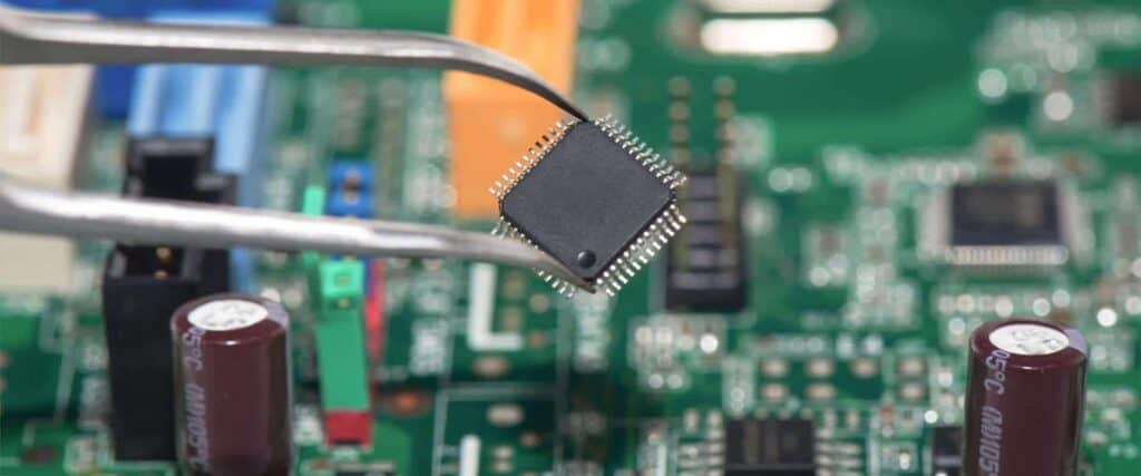
Assembly
Assembly is the process of soldering electronic components onto the fabricated PCB. This may be done by hand for prototyping or using automated pick-and-place and reflow soldering at scale.
Inspection and Testing
PCBs undergo electrical testing and optical inspection during assembly to catch defects. Automated optical inspection uses cameras to check for missing or misaligned components.
Box Build
The box build phase integrates the fully assembled and tested PCBs into the overall product enclosure with additional components and interconnects.
Choosing the Right PCB Materials
Selecting suitable materials is crucial for optimizing PCB performance, reliability, and manufacturability.
| Material | Key Characteristics | Applications |
|---|---|---|
| FR-4 | Most common, cost-effective material. Good electrical performance. | Consumer electronics, digital circuits. |
| High-frequency FR-4 | Modified FR-4 with improved dielectric properties for high-speed signals. | High-speed digital, communications. |
| Polyimide | Extremely high thermal tolerance up to 350°C. Flexible. | Aerospace, military, automotive. |
| Rogers | High frequency, thermal performance. Expensive. | Radar, satellite, wireless infrastructure. |
| Aluminum | Excellent thermal conductivity. Allows bonding heatsinks. | High power electronics, LEDs. |
Choosing the Right PCB manufacturer
With so many PCB manufacturers to choose from, here are key factors to consider:
- Capabilities – Ensure they can fabricate your board’s complexity, layer count, materials, quantities, etc.
- Quality – Look for manufacturers with rigorous quality control and inspection. Ask for their defect rates.
- Cost – Get quotes from multiple manufacturers. Balance cost vs quality.
- Lead Times – Confirm standard and expedited lead times match your project needs.
- Supply Chain – Choose manufacturers with suppliers near your own to reduce shipping times and delays.
- Certifications – Leading manufacturers have ISO 9001 or other certifications indicating standardized quality processes.
- Customer Support – Good manufacturers provide engineering support during design, manufacturing, and address any issues.
- Legal Compliance – Choose manufacturers that comply with environmental regulations like RoHS and data/IP protection laws.
Conclusion
Well-designed PCBs require carefully integrating schematic capture, layout, component selection, analysis, and following manufacturing design rules. Working with a PCB manufacturer during design helps avoid manufacturability issues. With diligent attention to planning and design principles, almost any electronics product can be successfully realized into a high-quality, functional printed circuit board ready for mass production and commercial success.
Frequently Asked Questions
What are some key advantages of using a multi-layer PCB?
Some key advantages of using a multi-layer PCB with 4 or more layers include:
- Higher component density by allowing more intricate routing on inner layers.
- Accommodate higher speeds and more complex circuits.
- Shield sensitive signals from noise by routing them between ground planes.
- Simplify high current routing by using entire layers as power planes.
- Allow flexibility to route signals point-to-point for optimized impedance control.
How are vias constructed on multi-layer boards?
Vias provide electrical connections between different layers on multilayer PCBs. There are three main types:
- Through-hole vias go through the entire board from top to bottom layer.
- Blind vias connect an inner layer to only one outer layer.
- Buried vias connect two or more inner layers without connecting to the outer layers.
Vias consist of drilled holes plated with conductive material, usually copper, to make the interlayer connections. High density multi-layer boards may also use microvias with smaller diameters.
What are some best practices for effective PCB thermal management?
Some good thermal management techniques in PCB design include:
- Carefully placing heat generating components with enough spacing for airflow.
- Using copper fills connected to ground planes to help spread heat.
- Adding thermal vias underneath hot components to conduct heat to inner layers.
- Directly soldering components to exposed thermal pads on the board.
- Adding cutouts and airflow openings in the PCB to force air over components.
- Using thicker copper weights, up to 2 oz, to improve thermal conductivity.
- Allowing space for heat sinks and mechanical attachments where needed.
- Modeling the thermal performance using simulation tools like Ansys Icepak.
How are surface mount components handled differently from through-hole in PCB design?
The main differences in designing for surface mount versus through-hole components are:
- Surface mount footprints have matching pad sizes/spacings for the component lead pitch while through-hole uses plated holes.
- SMD pads are located on only the top or bottom side while through-hole spans both sides.
- SMDs allow higher density packing and components on both sides.
- Traces routing out of SMD pads escape on 2-layers while through-hole uses vias.
- Through-hole requires larger keepout zones for the component leads and hole drilling.
- Through-hole allows simpler board assembly while SMDs require pick-and-place and reflow soldering.
What file formats are commonly used for transferring PCB data?
Some common file formats used in PCB design data exchange include:
- Gerber – The standard format for board fabrication data such as copper layers, silkscreen, solder mask, drill files.
- ODB++ – Contains the full PCB design data for fabrication and assembly in a standardized format.
- IPC-2581 – An emerging format with detailed PCB fabrication, assembly, and test information.
- DXF – 2D CAD drawing file for transferring PCB outline and drafting layers.
- STEP – 3D mechanical CAD file format for transferring board models to enclosures.
- PDF – Widely supported for 2D documentation like assembly drawings.
- Netlist – Specifies component connectivity such as for importing into PCB tools.


0 Comments