In the ever-evolving world of wireless communication and electronic devices, antennas play a crucial role in enabling seamless transmission and reception of electromagnetic signals. Among the various types of antennas, printed circuit board (PCB) antennas have gained significant popularity due to their compact size, low cost, and ease of integration into electronic systems.
A PCB antenna is a type of antenna that is designed and fabricated directly on the printed circuit board itself, eliminating the need for separate, dedicated antenna components. These antennas leverage the conductive traces and layers of the PCB to create the necessary radiating elements and structures required for effective signal transmission and reception.
In this comprehensive article, we will explore the concept of PCB antennas, their types, design considerations, advantages, and applications, providing a deep understanding of this versatile and widely-used technology.
Types of PCB Antennas
PCB antennas come in various forms, each designed to meet specific requirements and operating conditions. The following are some of the most common types of PCB antennas:
1. Microstrip Patch Antennas
Microstrip patch antennas are among the most widely used PCB antennas. They consist of a conducting patch, typically made of copper, etched onto a dielectric substrate (the PCB itself). The patch acts as the radiating element, while the ground plane on the opposite side of the PCB acts as a reflector. These antennas are known for their low profile, ease of fabrication, and integration into PCBs.
2. Inverted-F Antennas (IFA)
Inverted-F antennas (IFA) are compact and versatile PCB antennas suitable for applications where space is limited. They consist of a planar radiating element resembling an inverted “F” shape, typically positioned perpendicular to the PCB ground plane. IFAs are commonly used in mobile devices, such as smartphones and tablets, due to their compact size and efficient performance.
3. Planar Inverted-F Antennas (PIFA)
Planar Inverted-F Antennas (PIFA) are variations of the IFA design, where the radiating element is positioned parallel to the ground plane, providing an even more compact form factor. PIFAs are widely used in mobile and portable devices, as well as in wireless local area network (WLAN) applications.
4. Monopole Antennas
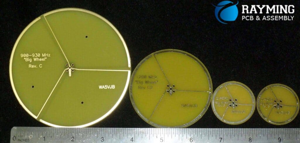
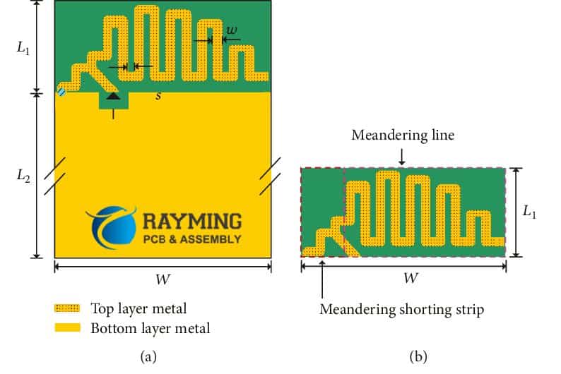
Monopole antennas are simple and versatile PCB antennas that consist of a single radiating element, typically a straight or meandered wire or trace, connected to the ground plane. They are known for their broadband performance and can be easily integrated into PCBs with various shapes and sizes.
5. Loop Antennas
Loop antennas, as the name suggests, feature a loop-shaped radiating element etched onto the PCB. They can be circular, rectangular, or other shapes, depending on the desired radiation pattern and operating frequency. Loop antennas are commonly used in radio-frequency identification (RFID) systems, near-field communication (NFC) devices, and wireless sensor networks.
6. Slot Antennas
Slot antennas are unique in that they are formed by cutting or etching a slot or aperture in the ground plane of the PCB. The slot acts as the radiating element, and the antenna’s performance can be tuned by modifying the shape and dimensions of the slot. Slot antennas are often used in wireless communication systems and radar applications.
7. Fractal Antennas
Fractal antennas are a class of PCB antennas that feature self-similar or fractal-like geometries in their radiating elements. These intricate designs allow for multi-band or wideband operation within a compact form factor. Fractal antennas are commonly used in modern wireless communication systems, where multiple frequency bands are utilized.
Design Considerations for PCB Antennas
When designing PCB antennas, several factors must be considered to ensure optimal performance, efficiency, and compatibility with the intended application. Here are some key design considerations:
1. Operating Frequency and Bandwidth
The operating frequency and required bandwidth are crucial factors that determine the size, shape, and design of the PCB antenna. Antennas must be designed to resonate at the desired frequency or frequency range, ensuring efficient radiation and reception of electromagnetic signals.
2. Radiation Pattern and Polarization
The radiation pattern and polarization of the PCB antenna should be carefully considered based on the application requirements. Different antenna types and designs exhibit distinct radiation patterns (omnidirectional, directional, etc.) and polarization characteristics (linear, circular, etc.), which can impact signal coverage and performance.
3. Impedance Matching
Impedance matching is essential for maximizing power transfer between the antenna and the transmission line or radio frequency (RF) circuitry. Proper impedance matching techniques, such as the use of matching networks or tuning elements, should be employed to minimize reflections and ensure efficient antenna operation.
4. PCB Substrate Properties
The properties of the PCB substrate, including dielectric constant, thickness, and loss tangent, play a significant role in the performance of the PCB antenna. These properties influence the antenna’s resonant frequency, bandwidth, and radiation efficiency, among other factors.
5. Ground Plane Size and Shape
The size and shape of the ground plane on the PCB can significantly impact the antenna’s performance. Larger ground planes generally improve antenna efficiency, while smaller ground planes may require additional design considerations or modifications.
6. Proximity to Other Components
The proximity of the PCB antenna to other components, such as metal enclosures, batteries, or shielding cans, can affect its radiation pattern and performance. Proper spacing and isolation techniques should be employed to minimize interference and optimize antenna performance.
7. Manufacturing Considerations
When designing PCB antennas, it is crucial to consider the manufacturing constraints and capabilities of the PCB fabrication process. Factors such as minimum trace widths, spacing, and copper plating thickness can impact the accuracy and reproducibility of the antenna design.
Advantages of PCB Antennas
PCB antennas offer numerous advantages over traditional, separate antenna components, making them an attractive choice for a wide range of applications:
- Integration and Miniaturization: PCB antennas can be directly integrated into the PCB design, eliminating the need for separate antenna components and enabling miniaturization of electronic devices.
- Cost-Effective: By leveraging the existing PCB manufacturing process, PCB antennas can be fabricated at a lower cost compared to dedicated antenna components, reducing overall system costs.
- Ease of Fabrication: PCB antennas can be etched or printed onto the PCB using standard PCB manufacturing techniques, simplifying the production process and reducing assembly complexity.
- Compact Form Factor: PCB antennas can be designed with various shapes and sizes, allowing for compact and space-efficient implementations in space-constrained applications.
- Robustness and Reliability: Being an integral part of the PCB, PCB antennas are less susceptible to mechanical damage or misalignment, improving overall system reliability.
- Design Flexibility: The ability to customize and optimize PCB antenna designs for specific applications and operating conditions provides design flexibility and performance optimization opportunities.
- Multi-Band and Wideband Capabilities: Through careful design and the use of advanced techniques, PCB antennas can be engineered to support multi-band or wideband operation, enabling versatile and future-proof wireless systems.
Applications of PCB Antennas
PCB antennas have found widespread applications in various industries and technologies due to their versatility, compact size, and cost-effectiveness. Some notable applications include:
- Mobile and Portable Devices: PCB antennas are extensively used in smartphones, tablets, laptops, and other portable electronics for wireless communication, GPS, Bluetooth, and Wi-Fi connectivity.
- Internet of Things (IoT) and Wireless Sensor Networks: The compact and low-cost nature of PCB antennas makes them ideal for IoT devices, wireless sensor nodes, and other embedded systems requiring wireless connectivity.
- Automotive and Transportation Systems: PCB antennas are employed in automotive electronics, such as keyless entry systems, tire pressure monitoring systems, and vehicle-to-vehicle (V2V) communication systems.
- Wearable and Biomedical Devices: The integration of PCB antennas into wearable devices and biomedical equipment enables wireless monitoring, data transmission, and remote healthcare applications.
- Radio-Frequency Identification (RFID): RFID systems often utilize PCB antennas for efficient communication between RFID readers and tags, enabling various applications such as asset tracking, inventory management, and access control.
- Military and Aerospace Applications: PCB antennas are employed in various military and aerospace systems, including communication systems, radar systems, and unmanned aerial vehicles (UAVs), due to their robustness and performance.
- Wireless Networking and Communication Systems: PCB antennas are used in wireless routers, access points, and other networking equipment for enabling wireless data communication and connectivity.
Design Tools and Simulation
To design and optimize PCB antennas, engineers and designers rely on various computer-aided design (CAD) tools and simulation software. These tools are essential for accurately modeling and predicting the performance of PCB antennas before physical prototyping and testing.
- Electromagnetic Simulation Software: Specialized electromagnetic simulation software, such as ANSYS HFSS, CST Microwave Studio, or Keysight EMPro, is used to model and analyze the electromagnetic behavior of PCB antennas. These tools employ numerical methods, such as the finite element method (FEM) or the method of moments (MoM), to simulate and optimize antenna designs.
- Circuit Simulation and Co-Simulation: Circuit simulation tools, like Keysight ADS or Cadence Virtuoso, are often used in conjunction with electromagnetic simulation software to perform co-simulations. This approach allows for the analysis of the entire RF system, including the antenna, transmission lines, and associated circuitry.
- Scripting and Automation: Many design tools offer scripting capabilities or application programming interfaces (APIs) that enable the automation of design tasks, parametric studies, and optimization processes, streamlining the PCB antenna design workflow.
- Antenna Design Libraries and Templates: Some CAD tools and software packages provide pre-built antenna design libraries or templates, which can serve as starting points for PCB antenna design and customization.
- Layout and PCB Design Tools: Mainstream PCB design tools, such as Altium Designer, Cadence Allegro, or KiCad, are used for creating the physical layout of the PCB, including the antenna structures and associated components.
By leveraging these design tools and simulation software, engineers can accurately predict the performance of PCB antennas, optimize designs for specific requirements, and minimize the need for costly physical prototyping and testing cycles.
Challenges and Future Trends
While PCB antennas offer numerous advantages, their design and implementation also present several challenges that must be addressed:
- Interference and EMI/EMC: PCB antennas can be susceptible to electromagnetic interference (EMI) from nearby components or external sources, potentially affecting their performance and signal integrity. Proper shielding, grounding, and EMI/EMC mitigation techniques are required to ensure reliable operation.
- Bandwidth and Multi-Band Requirements: As wireless communication systems continue to evolve and support multiple frequency bands, the demand for wideband and multi-band PCB antennas increases, posing design challenges in terms of size, complexity, and performance trade-offs.
- Integration with Advanced Materials: The integration of PCB antennas with advanced materials, such as metamaterials or liquid crystal substrates, is an active area of research, aiming to enhance antenna performance, tunability, and miniaturization capabilities.
- Miniaturization and Compact Design: As electronic devices continue to shrink in size, the demand for even smaller and more compact PCB antennas grows, pushing the limits of conventional antenna design and requiring innovative solutions.
- Antenna-Circuit Co-Design: The co-design of PCB antennas and their associated RF circuits is becoming increasingly important to optimize overall system performance and ensure efficient power transfer between the antenna and the RF front-end.
- Additive Manufacturing and 3D Printing: The advent of additive manufacturing and 3D printing technologies opens up new possibilities for PCB antenna fabrication, allowing for more complex and conformal antenna designs that can be integrated into various shapes and structures.
- Reconfigurable and Tunable Antennas: Research is underway to develop reconfigurable and tunable PCB antennas that can dynamically adapt their operating characteristics, such as frequency, polarization, or radiation pattern, to meet the changing needs of wireless communication systems.
As the demand for wireless connectivity and high-performance communication systems continues to grow, the development of advanced PCB antenna technologies will play a crucial role in enabling compact, efficient, and versatile wireless solutions.
Frequently Asked Questions (FAQs)
- Can PCB antennas be used for both transmitting and receiving signals? Yes, PCB antennas can be used for both transmitting and receiving electromagnetic signals. They are reciprocal devices, meaning that their performance is the same for transmission and reception.
- How does the size of a PCB antenna affect its performance? The size of a PCB antenna is directly related to its operating frequency and bandwidth. Generally, larger antennas are required for lower frequencies, while smaller antennas can be used for higher frequencies. However, miniaturization techniques can be employed to reduce the physical size of PCB antennas while maintaining acceptable performance.
- Can PCB antennas be designed for multiple frequency bands? Yes, PCB antennas can be designed to operate in multiple frequency bands, either through careful shaping of the radiating elements or by employing advanced techniques like fractal geometries or frequency-selective surfaces. Multi-band PCB antennas are commonly used in modern wireless communication systems that support multiple frequency bands.
- What are the typical materials used for PCB antennas? PCB antennas are typically fabricated using the same materials as conventional PCBs, such as copper for the conductive traces and radiating elements, and dielectric substrates like FR-4 or polytetrafluoroethylene (PTFE). However, specialized materials like liquid crystal polymers or ceramics may be used for specific applications or performance requirements.
- How does the ground plane size affect the performance of a PCB antenna? The size of the ground plane on the PCB can significantly impact the performance of a PCB antenna. Generally, larger ground planes provide better antenna efficiency and radiation performance, while smaller ground planes may result in reduced efficiency and modified radiation patterns. Proper ground plane design is crucial for optimal antenna performance.
Conclusion
PCB antennas have revolutionized the way wireless communication and connectivity are integrated into electronic devices. By leveraging the existing PCB manufacturing process and materials, these antennas offer a cost-effective, compact, and versatile solution for a wide range of applications.
From microstrip patch antennas to fractal antennas, the diverse types of PCB antennas cater to various operating frequencies, bandwidth requirements, and form factors. Careful design considerations, such as operating frequency, radiation pattern, impedance matching, and substrate properties, are essential for optimizing the performance of PCB antennas.
The advantages of PCB antennas, including miniaturization, ease of fabrication, robustness, and design flexibility, have made them indispensable components in mobile and portable devices, IoT systems, automotive electronics, and wireless networking equipment.
As wireless technology continues to evolve, the demand for advanced PCB antenna designs capable of supporting multi-band operation, reconfigurability, and integration with novel materials will drive further research and innovation in this field.
By leveraging cutting-edge design tools, simulation software, and manufacturing techniques, engineers and researchers are pushing the boundaries of PCB antenna performance, enabling the development of more efficient, compact, and versatile wireless solutions.
Whether for consumer electronics, industrial applications, or cutting-edge research endeavors, PCB antennas will continue to play a pivotal role in enabling reliable and seamless wireless connectivity in our increasingly connected world.


0 Comments