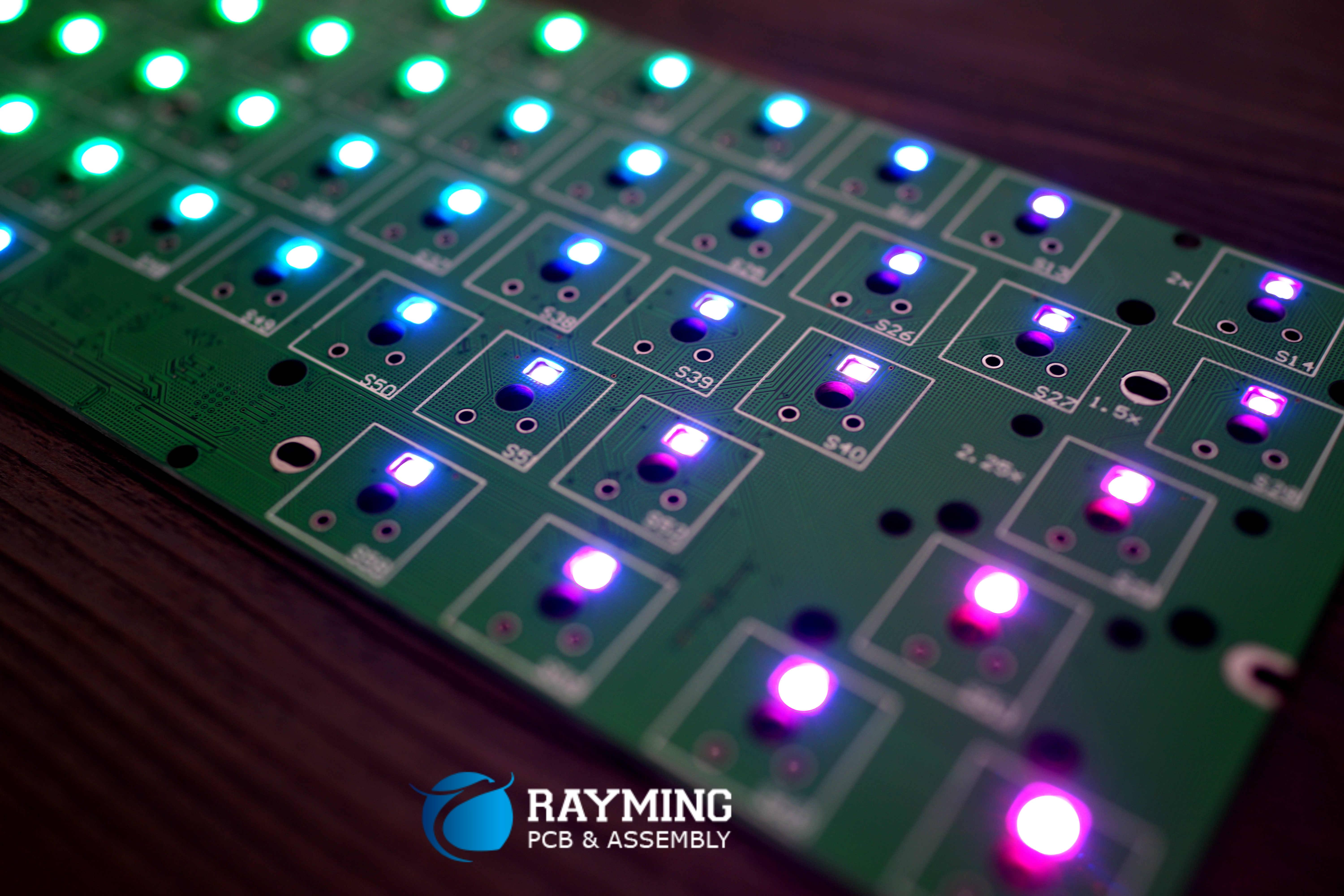
LEDs are increasingly used in lighting products due to their high efficiency, long lifetimes and eco-friendly nature. But designing the printed circuit board (PCB) that interconnects, powers and controls the LEDs requires careful consideration of electrical, thermal and mechanical factors for reliable functionality.
This comprehensive guide covers key design steps when making a custom PCB for LED lighting applications – from layout considerations, choice of materials to manufacturing and testing best practices. Factors like thermal management, high current capacities, driver electronics integration and optical element coupling are treated in detail. Let’s get started!
Specifying LED Requirements
The first step is determining the intended lighting application and corresponding choice of LEDs:
- Indoor Architectural Lighting
- Outdoor Lighting
- Automotive Lighting
- Signage or Display Lighting
Key LED parameters include:
- Luminous flux and efficiency
- Beam pattern and viewing angles
- Color temperature and CRI rating
- Peak wavelength and tolerance
- Maximum drive current rating
- Thermal characteristics
High power LEDs have integrated metal slug bases to conduct heat, but still need PCB cooling. Waterproofing treatments or secondary optics help weatherproofing.
Automotive LED lights require high reliability under vibrations and temperature cycling. Consider redundancy with parallel strings.
Estimating Power Requirements
The LED power supply requirements guide PCB design constraints like current rating, layer count and conductor widths able to support loads without overheating.
- Calculate total power based on LED ratings and desired luminous output
- Determine supply voltage – Typically 12V or 24V systems
- Derive maximum current from total power and voltage
For example, 100 1W LEDs with 120 lumen/Watt efficiency at 25% dimming in a 24V system need around 24V x 100 LEDs x 1W x 25% = 60 Watts. This corresponds to 60W/24V = 2.5A PCB current handling capability.
PCB Layout Considerations
PCB layout is critical is managing high currents through LEDs needing reasonable voltage drops. Use wide copper areas and multiple vias for power planes. Over 2 oz. copper thickness with minimum 0.4mm traces recommended with spacing for heat dissipation across layers.
- Locate drivers close to LEDs minimizing trace lengths
- Use symmetric placement for even current distribution
- LEDs and drivers need thermal reliefs and/or cutouts
- Enable visual inspection points to simplify troubleshooting
- Break out connectors/points allowing modular replacements
Thermal Management Strategies
The PCB provides primary heat sinking taking heat from LED junction to board and then onto external cooling elements like heat pipes and aluminium extrusions.
Common techniques include:
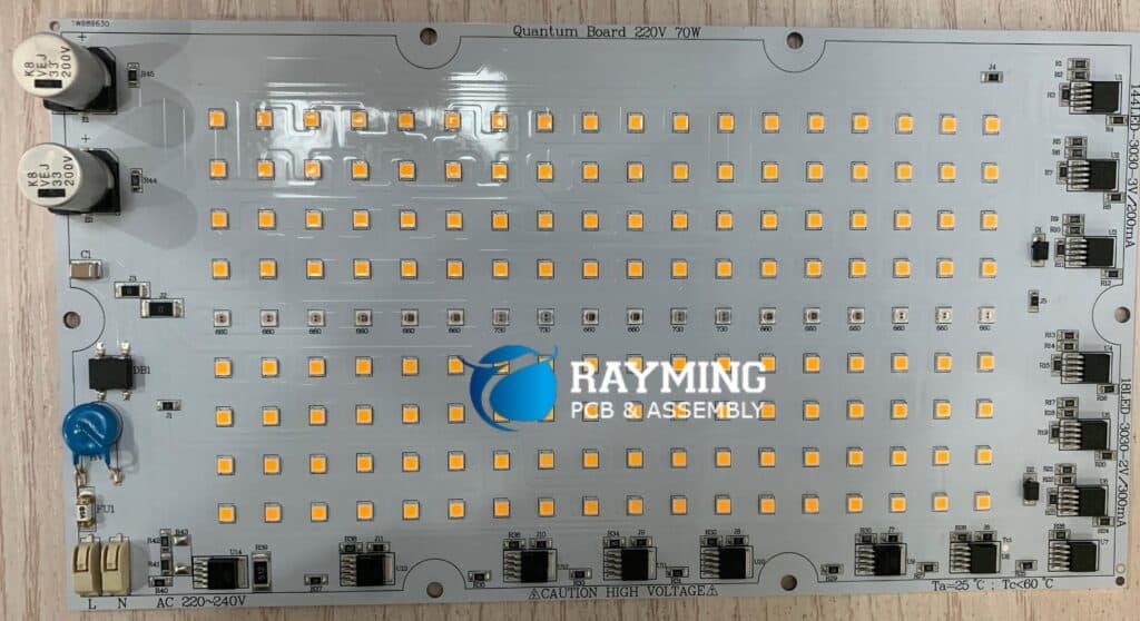
- Metal Core PCBs like aluminium or copper boards directly couple to LED slugs
- Thick copper layers serving as spreading planes
- Thermal vias conduct heat between layers
- Internal cutouts allowing air or liquid cooling
- External heat sinks like extruded fins augment cooling
- Use thermally conductive pad materials under LEDs
Keeping junction temperature under 80°C improves LED reliability over thousands of hours.
PCB Material Selection
Most LED lighting PCBs use standard FR-4 laminates, but certain applications benefit from specialized materials.
PCB Material Selection Considerations for LED Applications
| Parameter | Ideal Properties |
|---|---|
| Thermal conductivity | High for heat spreading (>4 W/mK) |
| Temperature range | Wide operating span (-40°C to +125°C rating) |
| Coefficient of thermal expansion | Matched to LEDs and metals |
| Dielectric strength | Withstand LED drive voltages |
| Flame resistance | UL94 V-0 for safety |
Consider ceramic filled composites or polyimide for high temp automotive lighting. Halogen free, low smoke laminates improve safety.
PCB Manufacturing Processes
Standard PCB fabrications processes suffice for most LED lighting boards:
- Lamination heat and pressure binds conductive layers
- Drilling creates plated through-holes for vias
- Copper Plating defines traces and fills holes
- Solder mask insulation prevents shorts
- Silkscreen applies markings
- Panelization supports mass production
- Assembly attaches components by soldering
- Testing validates boards prior to shipment
Thicker multi-layer boards over 2mm require stepped drilling. Beveled edge plating facilitates coating of cut board edges.
LED Integration Techniques
Robust integration of LED components onto PCBs ensures reliability:
- Through-hole LED pins soldered requiring correct iron temperature
- Surface mount LEDs reflowed using solder paste
- Underfill material helps strengthen component adherence
- Conformal coating protects against environmental factors
- Silicone gel fillers improve optical transmission
- Screw terminals allow pluggable replacements
- Human-computer interaction testing evaluates ergonomics
Automated optical inspection validates acceptability of production units.
LED Driver Integration
The PCB needs to incorporate DC-DC LED driver ICs providing controlled current source. Key considerations for driver integration:
LED Driver PCB Design Considerations
| Parameter | Guidelines |
|---|---|
| Driver power dissipation | Provide sufficient copper area, airflow and thermal vias |
| Input/Output filter capacitors | Low ESR types, positioned close to driver |
| Feedback sensing | Kelvin connect for accurate control |
| EMI management | Ground plane, Ferrite beads |
| High voltage insulation | Sufficient creepage distances |
| Protection devices | OVP, OCP, ESD protection |
Having integrated current setting resistors helps factory adjustment of currents.
Optical Considerations
To maximize application lighting performance, optical factors require consideration:
- Minimize shadowing elements in light path
- Ensure solder refracts light at correct angles
- Use white solder masks to reflect escaping light
- Diffusers and secondary lenses attach securely
- Reflector wells can surround emitters
- Protect external lenses through mechanical features
On-axis intensity and beam distribution characteristics should validate against photometric simulation models accounting for optical elements.
Design for Manufacturing
Following design for manufacturing guidelines during layout streamlines PCB fabrication and assembly:
- Allow sufficient tolerances for alignment and contacting
- Enable shared holes and edges to simplify fixturing
- Standardize footprints, cutouts and via styles
- Reuse circuits for multiple LED strings
- Comply with applicable light standards like UL 8750
These best practices reduce manufacturing issues and speed up processing.
Testing and Certification
Verifying quality requires different testing methods across production:
- Incoming inspection of PCBs checks for defects
- In-circuit testing validates shorts during assembly
- Burn-in testing eliminates infant mortalities running boards at elevated temperature, voltage and vibration levels
- Photometric testing measures light output and beam distributions in integrating spheres against simulated models
- Lifetime testing ages subset of boards to validate durability
- Safety testing determines adherence to required certifications like IEC/UL 62368 prior to sale
Rigorous testing protocols ensure long term reliability in the field across thousands of operating hours.
Conclusion
Designing reliable and cost-effective LED lighting PCBs requires attention to electrical, thermal, optical and mechanical elements through staged research, analysis, prototyping and process refinement balancing tradeoffs. With sound component selection, circuit design, layout considerations and verification testing, custom PCBs enable high performance LED luminaires meeting efficiency, lifetime and quality goals. Careful design enables sustainable LED lighting deployment at scale across infrastructure lighting, automotive and specialty use cases – saving energy globally.
Frequently Asked Questions
What is the function of the metal core PCB used in LEDs?
Metal core PCBs fabricated with thick aluminium or copper layers conduct heat from LED junctions efficiently across the board surface keeping temperatures low for higher reliability and light output. This enables high density LED placement.
What adhesive is used to mount LEDs onto MCPCBs?
Thermally conductive epoxy adhesives securely fasten surface mount LED packages onto metal core PCBs effectively transferring heat from the LED pads into the metal layer while providing superior mechanical adhesion strength under environmental stresses.
What is the difference between a LED driver and driver IC?
An LED driver refers to a full power supply unit that converts AC mains voltage into controlled DC current to power LED strings. An LED driver IC constitutes the critical PWM controller component within the driver that sets the correct constant current levels based on feedback.
How does underfill material enhance LED reliability?
Dispensing epoxy-based underfills between LED emitters and the PCB increases mechanical adhesion and withstands cyclic thermal stresses from expansion/contraction mismatches between different material interfaces – preventing LED detachment or solder cracking over product lifetime.
Why can’t through-hole LEDs withstand wave soldering?
Exposing the entire LED package and epoxy lens to molten wave solder can thermally shock and crack LED components. The high peak temperatures also degrade integrated optics permanently reducing light output. SMT LEDs reflowed locally avoid these risks.


0 Comments