Introduction
Printed circuit board (PCB) assembly is the process of soldering electronic components onto a PCB. One of the most critical steps in PCB assembly is applying solder paste onto the PCB pads and holes prior to component placement. This is done using a metal stencil that contains apertures matching the pads and holes on the PCB. The solder paste is applied onto the stencil, which transfers it onto the PCB when the stencil is placed over the board and a squeegee spreads the paste across the surface. Proper stencil design, solder paste application, and stencil cleaning are essential for high-quality and reliable PCB assemblies. This article provides a comprehensive guide to stencil PCB assembly.
Stencil Design Basics
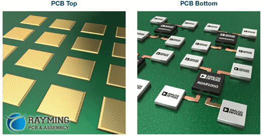
The stencil is a thin metal sheet laser-cut with apertures that match the pads, vias, and other features on the PCB. Good stencil design is critical for achieving accurate and consistent solder paste deposition. Here are some key stencil design considerations:
Aperture Shapes and Sizes
- Apertures are generally designed to match the copper pad size and shape.
- For fine-pitch components, the aperture size may need to be reduced to control solder paste volume.
- The aperture should allow adequate solder paste release onto the PCB pad.
Solder Mask Openings (SMO)
- The apertures must align properly with the solder mask openings on the PCB.
- Any misalignment can lead to solder bridges or insufficient paste volume.
Stencil Thickness
- Typical thickness ranges from 100-150μm (4-6 mil). Thicker stencils allow more paste volume.
- For fine pitch designs, thinner stencils of 50-75μm (2-3 mil) may be used.
Stencil Mounting/Framing
- The stencil frame design should provide good support and flatness across the stencil surface.
- This ensures consistent contact with the PCB during printing.
Other Features
- Fiducials, pin holes, and other features aid in aligning the stencil to the PCB.
Solder Paste Materials
Solder paste is a homogeneous mixture of solder alloy powder, flux, and binding agents that enables solder deposition by printing. The key considerations in solder paste selection include:
- Alloy composition – SAC alloys (Sn/Ag/Cu) are most common. Other options are Sn/Pb or Sn/Ag.
- Metal powder size – For fine-pitch printing, Type 4 or 5 powder (15-25μm particles) is preferred.
- Flux type – No-clean flux is widely used today and leaves benign residues. Halide-free fluxes improve reliability.
- Slump properties – Good viscosity and tackiness is needed to control slump after printing.
- Shelf life – 6 to 9 months at refrigerated temperatures.
| Solder Paste Types | Description |
|---|---|
| Type 3 | Larger particles, lower metal load, suitable for larger features |
| Type 4 | Smaller particles, moderate metal load, for 0.4-0.5mm pitch |
| Type 5 | Extra-fine particle size, higher metal load, for <0.4mm pitch |
High-quality solder paste matched to the PCB design is crucial for good print definition and solder joint formation.
Stencil Printing Process
The stencil printing process entails several steps to accurately transfer solder paste onto the PCB:
Stencil Cleaning
- Clean stencil thoroughly before use to remove any residues from prior prints.
- Dry cleaning followed by wipe with solder paste cleaner.
Stencil Mounting
- Align and mount the stencil on the printer carefully using mounting tools.
- Apply uniform frame tension for a flat stencil surface.
PCB Alignment
- Align the PCB to the stencil using board supports and fiducials.
- Maintain proper separation between PCB and stencil.
Solder Paste Application
- Roll solder paste across stencil surface using roller or squeegee to fill apertures.
- Apply even pressure and speed for uniform paste transfer.
Print Stroke
- Lower and raise the stencil with a smooth, steady motion to print the paste onto pads.
- Use print speeds of 25-100mm/sec depending on pitch.
Stencil Underside Cleaning
- Wipe the stencil underside during prints to remove excess paste.
- Prevent paste buildup and clogging of apertures.
Final Cleaning
- Clean the stencil thoroughly after the print run is completed.
- Removes all residual solder paste from that batch.
Proper printer setup, stencil tensioning, and consistent motion during print strokes are key to high-yield stencil printing.
Solder Paste Inspection
Solder paste inspection (SPI) after printing validates the paste deposits before component placement. SPI involves:
- 2D inspection – Checks for presence of paste, volume, and alignment.
- 3D inspection – Laser triangulation to measure paste height and shape.
Key SPI checks include:
- Aperture voids – Missing paste in stencil openings.
- Insufficient paste – Low paste volume on pads.
- Solder beads/blobs – Excess paste around pads.
- Smearing – Paste deposited outside of apertures.
- Height and area defects – Detects inadequate print transfer.
SPI provides critical feedback on stencil and printer performance. It identifies defects early to prevent assembly issues down the line.
Stencil Cleaning and Maintenance
As solder paste residues build up on stencils over multiple prints, stencil cleaning becomes very important. Key aspects are:
- Dry wiping – Use an initial dry wipe to remove most bulk paste residues.
- Wet cleaning – Use solder paste cleaners compatible with the paste flux to dissolve any remaining residues.
- Frequency – Clean stencil at least every 8 hours of production or 30 prints.
- Storage – Store stencils in a clean, dry environment in rigid frames.
- Nano-coating – Apply hydrophobic nano-coatings to reduce paste adhesion and ease cleaning.
- Stencil life – Typical stencil life is around 500 prints. Inspect regularly for wear, damage, or clogging.
Proper stencil cleaning and maintenance improves paste transfer consistency and stencil life. It is an essential step in any stencil printing process.
Optimizing the Stencil Printing Process
To achieve high print quality and yield, the stencil printing process needs continuous optimization through:
- Review of SPI defect data to identify problem areas.
- Analysis of prints and solder joints to find process gaps.
- Fine-tuning aperture sizes based on paste volume studies.
- Adjustments to printer parameters like print speed, separation distance, pressure.
- Improving stencil cleaning procedures and cycle times.
- Stencil design modifications if needed.
The various factors involved necessitate an iterative optimization approach based on results analysis. A well-dialed-in stencil printing process is crucial for reliable PCB assembly.
FQA
What are some key advantages of stencil printing for solder paste deposition?
Some key advantages of stencil printing are:
- Ability to print solder paste accurately and quickly onto PCBs with tight tolerances and fine features.
- Provides consistent solder paste volumes crucial for robust solder joints.
- Scalable and cost-effective method for high-volume PCB assembly.
- Mature process with availability of high-precision laser-cut stencils and advanced printers.
- Non-contact deposition prevents solder balling or mid-chip solder beads.
- Widely adopted process with established inspection, maintenance, and optimization techniques.
How does one determine the optimal solder paste print speed?
Print speed is optimized by considering factors like stencil and aperture size, pitch between pads, separation distance of stencil from PCB, and solder paste rheology. Typical print speeds range from 25-100mm/sec. Slower speeds around 25-50mm/sec are used for ultra-fine pitch printing to allow adequate paste release. Higher speeds of 75-100mm/sec can be used for less demanding designs. Print trials are done to assess paste transfer at different speeds based on SPI and solder joint inspection. The optimal speed is chosen to reliably deposit the required paste volume at the desired print definition.
Why is it important to do solder paste inspection (SPI) after stencil printing?
SPI is critical because it provides early detection of any solder paste printing defects before assembly proceeds further. It can identify problems like insufficient paste deposits, smearing, clogged apertures, etc. If these issues are not caught early, they can lead to solder opens, shorts, missing joints during reflow soldering. This negatively impacts product yield and reliability. Conducting SPI and taking corrective actions to fix issues prevents propagation of defects to downstream assembly processes.
How often should stencils be cleaned during production?
As a general rule, stencils should be cleaned at least every 8 hours of production printing time or after every 30 print runs. More frequent cleaning may be needed for ultra-fine pitch patterns. Insufficient cleaning allows paste residues to accumulate and clog apertures. It reduces print accuracy and quality over time. Frequent cleaning maintains aperture integrity and paste transfer consistency, preventing progressive print defects. Stencil cleaning cycle time can be optimized based on factors like stencil area, pitch, residue buildup rate, and cleaning efficacy.
What are some best practices for stencil storage and maintenance?
Recommended stencil storage and maintenance practices include:
- Store stencils in a dedicated, controlled environment away from dust or contamination.
- Keep stencils framed and tensioned to prevent warpage.
- Clean stencils thoroughly and apply anti-tack coating for storage.
- Inspect stencils regularly under microscope for any signs of wear, damage or clogging.
- Replace stencils once they exceed recommended life cycles or show cleaning difficulty.
- Keep detailed logs of stencil inventory, usage, cleaning logs, inspections, etc.
- Handle stencils carefully to prevent bending, denting or aperture clogging during usage and storage.
Following these best practices maximizes stencil life, print consistency, and process control during stencil PCB assembly.
Conclusion
Stencil printing is an indispensable process in electronics manufacturing for accurate and repeatable solder paste deposition onto PCBs. A high-quality stencil matched to the PCB design characteristics along with a well-controlled printing process and frequent stencil maintenance is key to achieving consistent, high-yield solder joints. As PCB components get smaller and densities increase, stencil technology and materials continue to evolve accordingly. The guidelines provided in this article can help build expertise in stencil printing to implement a robust assembly process for a wide range of product types. With sufficient process controls and ongoing optimization, stencil printing will continue to enable miniaturization and advancement across the electronics industry.


0 Comments