Introduction to Printed Circuit Boards and Their Manufacturing
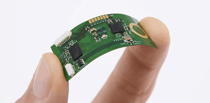
A printed circuit board (PCB) is the backbone of an electronic device. It provides the necessary electrical connections between components to form a functional product. PCB assembly, also known as PCBA, is the process of soldering electronic components onto a PCB. Proper printed circuit assembly is essential for creating a high-quality and reliable end product. This article will provide a comprehensive overview of PCB assembly, examining key aspects like materials, manufacturing processes, defect inspection, and frequently asked questions.
PCB Materials and Components
The PCB itself is made up of different materials laminated together:
Substrate Materials
This forms the base of the board and provides mechanical support. Typical materials used are:
- FR-4 Glass Epoxy – Most common rigid PCB material
- CEM-1/3 Composite Epoxy Material – High frequency applications
- Polyimide – Flexible PCBs
- Ceramics – High thermal/performance applications
Conductive Materials
These provide the electrical connectivity traces on the PCB. Common examples are:
- Copper – Most common conductive material
- Aluminum – Lower cost but higher resistance
- Gold – Used for coating to prevent corrosion
Solder Mask
A coat of insulative lacquer applied on top of the copper traces, leaving only the solder pads exposed. This prevents solder bridges from forming between closely spaced traces.
Silkscreen
Used to print reference designators, polarity indicators, board outlines etc. Helps identify components during assembly and debugging.
In addition to the board itself, electronic components are soldered on during PCBA. Components include:
- Active components – ICs, transistors
- Passive components – Resistors, capacitors, diodes
- Electromechanical – Switches, relays, connectors
- PCB assemblies may also utilize other materials like conformal coating.
Manufacturing Processes
There are several key steps involved in assembling components onto a PCB:
1. Solder Paste Printing
Solder paste containing spherical solder alloy particles mixed with flux is applied on to the PCB pads where components will be placed. This is done using stencils and solder paste printers.
2. Component Placement
Components are accurately placed on their designated pads on the PCB. This is done manually for low volume assembly, while automated pick and place machines are used for mass production.
3. Solder Reflow
The PCB assembly is passed through a reflow oven with a temperature profile optimized to melt the solder paste and form solder joints.
| Stage | Profile | Purpose |
|---|---|---|
| Preheating | 30-60 secs @ 150-180°C | Gradually bring assembly to reflow temperature |
| Thermal soak | 60-120 secs @ 180-220°C | Activate flux, evaporate volatiles |
| Reflow peak | 20-40 secs @ 230-260°C | Melt solder paste to form joint |
| Cooling | 2-6 mins to drop to room temp | Controlled cooling to prevent defects |
4. Cleaning
Residual flux on the assembly is cleaned using appropriate cleaning agents. This removes potential corrosive residues.
5. Inspection
PCB assemblies are visually inspected for any defects in the soldering process. Automated optical inspection (AOI) systems may also be utilized.
6. Testing
PCB assemblies undergo electrical testing like in-circuit tests to validate functionality.
Quality Control and Defect Prevention
Maintaining quality in PCB assembly involves identification and mitigation of potential defects. Some key aspects:
- Process control – Ensuring assembly process parameters like temperature profiles are optimized and tightly controlled. This prevents issues like cold solder joints.
- Materials management – Proper storage/handling of sensitive materials like solder paste avoids defects from contamination or variation.
- Inspection – Critical to catch errors so corrections can be made prior to further assembly/testing. Done at multiple stages of the process.
- Training – Well trained operators, especially for manual operations like component placement, are needed for quality and consistency.
- ESD control – Use of proper grounding/ionization to avoid electrostatic discharge damage to sensitive components.
- Traceability – Part serialization and production data tracking allows tracing a defect to a specific batch/time/machine etc.
By implementing robust quality practices per IPC standards, PCB assemblers can maximize yield and reliability of the end product.
Frequently Asked Questions
Here are some common questions regarding printed circuit board assembly:
Q: What is the difference between PCB fabrication and PCB assembly?
A: PCB fabrication involves creating the bare printed circuit board. PCB assembly is about soldering electronic components onto the fabricated PCB.
Q: Are components mounted only on one side or both sides of a PCB?
A: A PCB can have components mounted on a single side or on both sides. Multilayer boards allow components on outer and inner layers.
Q: How are very small SMT components mounted accurately on boards?
A: High precision pick-and-place machines with computerized vision systems are used to place tiny SMT components onto PCBs.
Q: What types of testing are done on assembled PCBs?
A: Common testing methods include in-circuit test (ICT), flying probe testing, boundary scan, and functional/environmental stress testing.
Q: Which software tools are used in PCB assembly?
A: CAD tools for board design, CAM tools for manufacturing, solder paste inspection tools, PCBA documentation tools etc. are commonly used.
Conclusion
In summary, printed circuit board assembly is a complex, multistep manufacturing process that requires expertise and precision to produce a high-quality electronic product. Careful material selection, process control, defect prevention, inspection and testing are crucial. When executed proficiently, PCBA delivers a robust, reliable PCB ready for integration into electronic devices and gadgets. The demand for economical, high-tech PCBs is driving rapid advances in PCB assembly technology and capabilities.


0 Comments