Introduction to PCBs
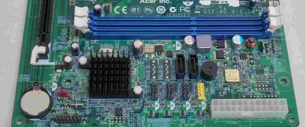
A printed circuit board (PCB) is the foundation of an electronic device, providing mechanical support and electrical connections between components. PCBs contain conductive traces etched from copper sheets and laminated onto a non-conductive substrate. Electronic components are soldered to pads on the PCB to create a functional circuit.
The fabrication and assembly process transforms a PCB design into a finished board ready for installation. Careful attention during PCB manufacturing is critical for producing boards that function reliably over the product lifetime. This guide covers key considerations for making quality PCBs.
PCB Design
The PCB design process establishes the board layout, copper traces, and component footprints. While designers often use CAD software like Altium, KiCad, or Eagle for PCB design, several factors impact fabrication and assembly:
Layer Stackup
The layer stackup defines the number of copper layers and the order of dielectric substrates in the PCB. Simple boards may only use a single-sided or double-sided layer stackup. High density designs require more layers – up to 30+ for advanced boards.
Trace Width/Spacing
The trace width and spacing set the density of routed connections on a PCB layer. Thinner, more tightly spaced traces allow greater interconnection but increase fabrication difficulty.
Via Construction
Vias provide vertical connections between layers in multilayer PCBs. Their diameter, plating, and density affect manufacturing.
Component Footprints
The component footprints specify the land patterns for soldering parts. Appropriate footprint design ensures adequate solder joint strength.
Board Outline and Shape
The PCB outline and shape impacts panel utilization efficiency during fabrication. Complex board shapes can also create challenges for routing traces.
Finish Requirements
Special finishes like immersion silver, ENIG, or OSP may be required for certain applications or soldering processes. The finish adds cost and affects fabrication processing.
Other Requirements
Designers may impose special requirements like impedance control, press-fit connectors, buried/blind vias, heavy copper, controlled dielectric materials, etc. These can constrain fabrication options.
Manufacturing Standards
Adhering to IPC standards for trace/space, hole size, annular rings, etc. enables manufacturers to produce the board reliably.
Prototyping vs Production
During development, designers may use simplified designs and low-cost prototyping services. However, designs should be refined before volume production to avoid issues:
Prototyping
- Relaxed design rules and standards
- Limited fabrication capabilities
- Small quantities
- May lack solder mask, legend, etc.
Production
- Tight design rules and standards
- Advanced manufacturing capabilities
- Large quantities
- Full solder mask, legend, surface finish, etc.
If designs are not properly updated before production, it can lead to delays, unreliability, and added costs.
Selecting a PCB Manufacturer
Choosing the right PCB manufacturer is critical for achieving high quality boards. Key factors in selecting a fabrication partner include:
Capability Analysis
Evaluate manufacturers based on their capabilities – available layers, line/space tolerances, hole sizes, finishes, etc. Ensure they can fabricate your design reliably.
Quality Systems
Look for manufacturers with quality systems like ISO 9001 certification. This indicates they follow documented procedures and conduct inspections.
Supply Chain Management
Ask about their supply chain management. Do they own their own factories or use contracted partners? How is yield monitored?
Engineering Support
Many issues arise during transferring designs to fabrication. Choose a manufacturer who provides engineering review and DFM analysis as part of their standard pre-production process.
Prices and Lead Times
Understand the manufacturer’s standard lead times and pricing model. Be cautious of extremely low prices or short lead times, which may indicate risk.
Communication and Responsiveness
You will likely exchange many questions and files during fabrication. Select a highly communicative manufacturer who responds quickly.
Order Documentation
Manufacturers require a set of documentation to build each PCB order accurately:
- Gerber Files: Standard file format for PCB fabrication data
- Bill of Materials: List of components for assembly
- Assembly Drawings: Diagrams showing component placement and solder joints
- Board Specification: Defines build requirements – layers, finish, tolerances, testing, etc.
- Fabrication Notes: Design warnings, clarifications, or special instructions
Thorough documentation reduces ambiguity, ensuring the manufacturer constructs your boards correctly.
Fabrication Process Steps
Printed circuit boards pass through a series of complex processes during fabrication. While exact sequences vary between factories, typical PCB fabrication includes:
Imaging
The design layout data is patterned onto the conductive copper foil. Photoresist is either exposed with UV light or directly imaged.
Etching
Exposed copper is etched away, leaving only the protected traces and pads. Foils, photoresist, and etchants are chemically stripped.
Lamination
Core layers are arranged in the proper stackup order and fused together under heat and pressure. Prepregs bond the cores.
Drilling
Higher layers require interconnecting vias. Holes are precisely drilled through the board with small diameter bits. The walls are plated.
Metallization
Copper is plated onto drilled hole walls and surface pads, electrically connecting between layers.
Solder Mask
The solder mask insulates exposed copper from solder and the environment. Openings permit soldering.
Silkscreen
Silkscreen printing applies board nomenclature like reference designators.
Surface Finish
A chemical coating such as immersion silver or OSP is applied to protect exposed pads and traces.
Electrical Test
Bare boards are electrically tested against shorts, opens, impedance, etc. to validate quality.
Inspection
Optical inspection and AOI systems check for defects in the boards. Acceptable boards proceed.
Panelization
Individual PCBs are routed from larger fabrication panels for shipment and assembly.
While simplifying, the list demonstrates the challenging intricacies of PCB manufacturing. Each step must be carefully controlled to produce functional boards.
Solder Paste Stencil Fabrication
Solder stencils are required for applying paste during PCB assembly. Like the board itself, the stencil demands careful fabrication:
Laser Cutting
A CO2 laser cuts the stencil pattern into the metal foil – typically stainless steel or nickel alloy.
Electropolishing
The cutting process leaves small burrs. Electropolishing removes these to create clean aperture walls.
Cleaning
Chemical cleaning strips oils and debris from fabrication. This prevents contamination of the solder paste.
Framing
The foil is mounted into a metal frame to provide rigidity. Auto-release options allow easy stencil removal after paste application.
Inspection
Microscopes check aperture dimensions and walls for defects. Touch pin probes electrically verify pattern completeness.
High precision is vital – solder paste bricks on the board mirror issues with the stencil. Any defects degrade soldering quality.
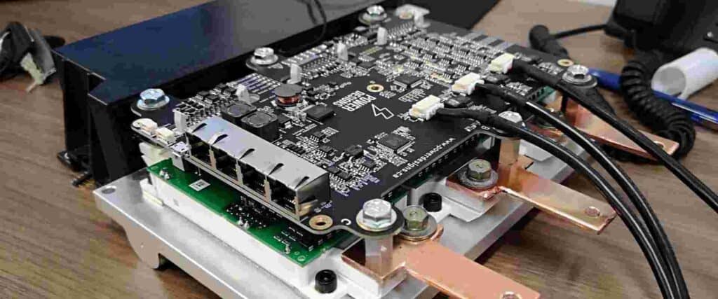
Assembly Process Overview
Once fabricated boards and stencils are received, the PCB moves into assembly. This involves soldering components onto the boards. Typical assembly steps include:
Solder Paste Printing
The stencil is aligned over the PCB and solder paste is squeegeed over the stencil. This deposits droplets onto attachment pads.
Pick and Place
Robotic pick and place machines populate components onto the paste. Vision systems align parts precisely.
Reflow Soldering
The boards pass through a reflow oven to heat the solder paste above liquidus. The paste forms reliable solder joints.
Inspection
Assembled boards undergo optical, x-ray, or automated optical inspection to check for defects like missing components, tombstones, bridges, etc. Issues are reworked.
Conformal Coating
A protective coating may be applied to shield against moisture, debris, chemicals, etc.
Programming/Functional Test
For boards containing a microprocessor, firmware is loaded and functional tests exercised to validate performance.
Final Inspection
Detailed workmanship inspections use magnifying lenses to check solder joints, cleanliness, markings, etc. prior to shipment.
Achieving High Soldering Quality
Producing robust, reliable solder joints demands paying attention to:
Solder Paste
- Use high quality no-clean paste from reputable brands
- Match alloy to pad finish (SnPb, SAC305, etc.)
- Ensure even deposition using proper stenciling procedure
Stencil Design
- Add proper amount of solder paste per joint based on size and pitch
- Include offsets/chamfers to reduce bridging risk
- Nanocoat stencil for easy paste release
Component Placement
- Place smallest parts first with finer pitch machines
- Ensure sufficient accuracy and repeatability
Reflow Profile
- Tune oven zones to achieve target profile based on paste and parts
- Add soak zone to reduce solder balling
- Include proper cooling ramp rate
Inspection
- Verify joint shape, fillet presence, heel fillet, wetting, etc.
- Detect insufficient paste, tombstones, bridges, etc.
Paying attention to these parameters helps minimize assembly defects for maximum reliability. Consult process experts and inspect samples under magnification.
Common PCB Assembly Challenges
Despite best efforts, issues can arise during PCB assembly:
| Problem | Potential Causes | Prevention |
|---|---|---|
| Solder Shorts | Excess paste deposition, close pad spacing | Optimize stencil design, inspect paste print |
| Solder Balling | Poor paste, rapid reflow ramp | Tune profile, use correct paste |
| Tombstones | Misaligned parts, uneven paste | Increase accuracy, clean paste off pads |
| Voids | Poor wetting, outgassing flux | Use higher activity flux, remove contaminants |
| Bridges | Too much paste between pads | Reduce stencil aperture size for dense footprints |
| Cold Solder Joints | Insufficient heat, slow ramp | Increase peak temp, extend time above liquidus |
Thorough inspection at multiple steps helps detect and address assembly process deviations before they progress downstream.
X-Ray Inspection
X-ray imaging provides detailed inspection of component placement and solder joints hidden underneath packages. This reveals hidden defects:<div>
| Defect | Description |
|---|---|
| Insufficient paste | Too little solderpaste deposited on pad |
| Voiding | Air bubbles trapped in solidified joint |
| Cold / dull joint | Joint not fully melted and flowed |
| Head-in-pillow | Component body not aligned properly on pads |
| Bridging | Solder shorting between two pads |
| Foreign object | Contaminant trapped under component |
</div>
X-ray is especially useful for inspecting components like BGAs or QFNs with hidden solder joints. It can validate assembly quality before products ship.
Continuous Improvement
Achieving assembly excellence requires ongoing continuous improvement through:
- Statistical process control tracking
- Operator training/certification
- Regular machine maintenance
- Corrective actions from defects
- Design reviews to improve manufacturability
- Upgrading equipment and software
- Refining processes based on lessons learned
Assemblers should adopt a culture of quality where improvement is built into daily work. Validated processes, inspection data, and customer feedback help drive gains over time.
Conclusion
Producing robust, reliable PCBs requires close cooperation between designers, fabricators, and assemblers. Following best practices for design, documentation, manufacturing, inspection, and process control prevents defects and minimizes risks during volume production. Choosing reputable partners focused on quality is key to success. With diligent attention across the electronics supply chain, companies can bring their innovative products from prototypes to high yield manufacturing.
Frequently Asked Questions
What are some common PCB substrate materials?
FR-4 glass epoxy is the most common base material for rigid PCBs. Other options include CEM-1, FR-2, Rogers, polyimide, and aluminum for more demanding applications. Flexible PCBs use polyimide or polyester films.
What is HDI technology?
High density interconnect (HDI) refers to PCBs with trace/space less than 100 microns (0.1 mm), blind/buried vias, and microvias under 150 microns diameter. This provides routing density for complex ICs.
What is an impedance controlled PCB?
For high speed signals, PCBs may require controlled dielectric materials and trace dimensions to match target impedance – often 50 or 100 Ohms. This prevents signal reflection.
What are fiducials and their purpose?
Fiducials are reference markings on PCBs for aligning equipment like assembly robots. They provide accurate positional recognition between boards and stencils during soldering.
How can designers check manufacturing capability?
Fabricators can provide detailed capability reports listing their capabilities for layers, line width, vias, tolerances, solder masks, etc. Check that your design is within limits.


0 Comments