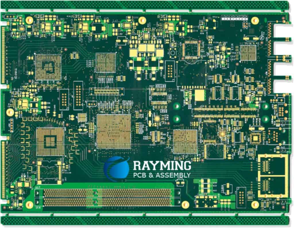
In the ever-evolving world of electronic systems, printed circuit boards (PCBs) have become increasingly complex and densely populated with components. As the demand for miniaturization, high-speed performance, and advanced functionality continues to grow, traditional single-layer or double-layer PCBs often fall short in meeting these requirements. This is where multilayer PCBs come into play, offering a sophisticated solution to address the challenges of modern electronics design.
A multilayer PCB is a printed circuit board that consists of multiple conductive layers, separated by insulating materials, and interconnected through strategically placed vias (plated or unplated holes). These additional layers provide more routing space, allowing for higher component density, improved signal integrity, and enhanced thermal management capabilities.
In this comprehensive article, we will explore the concept of multilayer PCBs, their construction, advantages, design considerations, applications, and manufacturing processes, shedding light on why these advanced PCBs are essential in today’s electronic landscape.
Construction and Materials
Multilayer PCBs are constructed using a combination of conductive layers, insulating materials, and interconnecting vias. The key components and materials involved in their construction are:
1. Conductive Layers
The conductive layers in a multilayer PCB are typically made of copper, although other materials such as aluminum or gold may be used in specialized applications. These layers are etched or deposited onto the insulating substrate, forming the desired circuit patterns, traces, and pads for component placement.
2. Insulating Materials
The insulating materials used in multilayer PCBs are commonly known as prepregs (pre-impregnated materials) or core materials. These materials provide electrical insulation between the conductive layers and mechanical support for the overall structure. Common insulating materials used in PCB construction include:
- FR-4 (Flame Retardant 4): A glass-reinforced epoxy laminate, widely used for its balance of electrical, mechanical, and thermal properties, as well as its cost-effectiveness.
- Polyimide: A high-temperature thermosetting polymer with excellent insulating properties and chemical resistance, often used in high-reliability applications.
- Rogers Materials: Specialized materials like RT/duroid and RO4000 series, designed for high-frequency and high-speed applications, with low dielectric loss and controlled impedance characteristics.
3. Vias
Vias are plated or unplated holes that provide electrical connections between different conductive layers in a multilayer PCB. They are crucial for routing signals, power, and ground planes across multiple layers. The most common types of vias include:
- Through-Hole Vias: These vias pass through all layers of the PCB, allowing for vertical interconnections.
- Buried Vias: These vias are completely buried within the PCB layers, connecting internal layers without extending to the outer surfaces.
- Blind Vias: Blind vias connect an outer layer to an internal layer, but do not extend through the entire thickness of the PCB.
4. Solder Mask and Silkscreen
Multilayer PCBs often incorporate a solder mask, which is a protective coating applied over the conductive layers, leaving only the component pads and specific areas exposed for soldering. Additionally, silkscreen markings are printed on the PCB’s surface to provide component designations, polarity indicators, and other useful information for assembly and maintenance.
Advantages of Multilayer PCBs
The adoption of multilayer PCBs in electronic systems offers numerous advantages over their single-layer or double-layer counterparts:
- Increased Component Density: With multiple conductive layers available, multilayer PCBs can accommodate a higher density of components, allowing for more compact and space-efficient designs.
- Improved Signal Integrity: By separating critical signals onto dedicated layers and incorporating shielding planes, multilayer PCBs minimize crosstalk, electromagnetic interference (EMI), and signal degradation, ensuring better signal integrity and system performance.
- Enhanced Thermal Management: Dedicated power and ground planes in multilayer PCBs can dissipate heat more effectively, reducing the risk of hot spots and improving overall thermal management.
- Reduced Trace Lengths: With more routing layers available, trace lengths can be minimized, reducing propagation delays, impedance mismatches, and signal reflections, particularly in high-speed and high-frequency applications.
- Increased Design Flexibility: Multilayer PCBs offer greater flexibility in routing signals, power, and ground planes, enabling more complex and optimized designs that would be challenging or impossible to achieve with fewer layers.
- Improved Electromagnetic Compatibility (EMC): The inclusion of dedicated shielding and ground planes in multilayer PCBs helps to minimize electromagnetic emissions and improve the overall EMC performance of the electronic system.
- Higher Reliability: The layered construction of multilayer PCBs provides increased mechanical stability and resistance to environmental factors, such as vibration, temperature fluctuations, and moisture, resulting in improved reliability and longer product lifespan.
Design Considerations for Multilayer PCBs
While multilayer PCBs offer numerous advantages, their design process involves additional complexities and considerations compared to single-layer or double-layer PCBs. Here are some key design factors to consider:
1. Layer Stackup
The layer stackup refers to the arrangement and sequence of conductive layers, insulating materials, and their thicknesses within the multilayer PCB structure. Proper layer stackup design is crucial for ensuring signal integrity, impedance control, thermal management, and manufacturability. Factors such as layer count, material selection, and layer assignments (e.g., signal layers, power planes, ground planes) must be carefully considered.
2. Signal Integrity and Impedance Control
In multilayer PCBs, signal integrity and impedance control become even more critical, especially for high-speed and high-frequency applications. Proper trace routing, layer assignments, and material selection are essential to maintain consistent impedance and minimize signal reflections, crosstalk, and electromagnetic interference.
3. Power Integrity and Decoupling
With multiple power and ground planes available, multilayer PCBs offer opportunities for effective power distribution and decoupling. Proper placement and routing of decoupling capacitors, as well as the design of power and ground planes, are crucial for maintaining stable power delivery and minimizing noise and voltage fluctuations.
4. Thermal Management
The increased component density and power dissipation in multilayer PCBs necessitate careful thermal management considerations. Dedicated thermal planes, thermal vias, and strategic component placement can help dissipate heat more effectively, preventing hot spots and ensuring reliable operation.
5. Manufacturing Considerations
Multilayer PCB design must take into account manufacturing constraints and capabilities, such as minimum trace widths, spacing, via sizes, and layer-to-layer registration tolerances. Close collaboration with PCB manufacturers and adherence to industry standards are essential to ensure manufacturability and yield.
6. Cost and Lead Time
Multilayer PCBs generally have higher manufacturing costs and longer lead times compared to their single-layer or double-layer counterparts. The number of layers, material selection, and design complexity can significantly impact the overall cost and production time.
Applications of Multilayer PCBs
Multilayer PCBs are widely used in a variety of applications across various industries, enabling advanced functionality, high performance, and miniaturization. Some notable applications include:
- Consumer Electronics: Smartphones, tablets, laptops, and other portable devices often employ multilayer PCBs to achieve high component density, efficient power distribution, and signal integrity for various interfaces and wireless communication protocols.
- Telecommunications: Multilayer PCBs are essential in telecommunication equipment, such as routers, switches, and base stations, where high-speed data transmission, signal integrity, and EMI shielding are critical requirements.
- Automotive Electronics: Advanced driver assistance systems (ADAS), infotainment systems, and other automotive electronics rely on multilayer PCBs to accommodate complex circuitry, ensure reliable operation in harsh environments, and meet stringent EMC regulations.
- Aerospace and Defense: Multilayer PCBs are used in avionics systems, radar equipment, and military electronics, where high reliability, durability, and advanced performance are paramount.
- Industrial Control Systems: Programmable logic controllers (PLCs), automation systems, and other industrial control equipment often utilize multilayer PCBs to accommodate complex circuitry, ensure signal integrity, and provide robust operation in harsh industrial environments.
- Medical Devices: From diagnostic equipment to implantable devices, multilayer PCBs are employed in the medical industry due to their ability to accommodate high component densities, provide effective shielding, and meet stringent regulatory requirements.
- Internet of Things (IoT) and Wearables: As IoT devices and wearable electronics become more compact and feature-rich, multilayer PCBs enable the integration of various sensors, wireless communication modules, and power management systems within a small form factor.
Manufacturing Process for Multilayer PCBs
The manufacturing process for multilayer PCBs is more complex than that of single-layer or double-layer PCBs, involving additional steps and specialized techniques. The general process flow for multilayer PCB manufacturing includes the following stages:
- Layer Fabrication: Individual conductive layers are fabricated by laminating copper foil onto insulating substrates, followed by photolithography and etching processes to create the desired circuit patterns.
- Layer Inspection and Quality Control: Each individual layer undergoes thorough inspection and testing to ensure compliance with design specifications and quality standards.
- Layer Registration and Alignment: Alignment tooling holes or fiducial marks are used to precisely align and register the individual layers during the lamination process.
- Lamination and Bonding: The individual layers, along with prepregs or core materials, are stacked and aligned according to the layer stackup design. This stack is then subjected to high temperature and pressure in a lamination press, bonding the layers together into a rigid multilayer structure.
- Drilling and Via Formation: After lamination, holes are drilled or punched through the multilayer structure for through-hole vias and component mounting. These holes are then plated with conductive materials, such as copper or gold, to form the interconnecting vias.
- Outer Layer Processing: The outer layers undergo additional processing steps, including photolithography, etching, solder mask application, and surface finishing (e.g., hot air solder leveling, immersion tin, or immersion silver).
- Electrical Testing: Comprehensive electrical testing is performed on the multilayer PCB to verify continuity, resistance, and functionality of the interconnections and circuit paths.
- Final Inspection and Quality Control: The finished multilayer PCB undergoes a final visual and dimensional inspection to ensure compliance with design specifications and quality standards.
Throughout the manufacturing process, strict quality control measures and adherence to industry standards, such as those set by the IPC (Association Connecting Electronics Industries), are essential to ensure the reliability and performance of the multilayer PCBs.
Emerging Trends and Future Developments
As electronic systems continue to evolve and demand higher performance, increased miniaturization, and advanced functionality, the development of multilayer PCB technology is also progressing. Here are some emerging trends and future developments in the field of multilayer PCBs:
- High-Density Interconnect (HDI) PCBs: HDI PCBs are a specialized type of multilayer PCBs that feature higher density interconnections, finer trace widths, and smaller via sizes. These advanced PCBs are designed to accommodate the ever-increasing component density and miniaturization requirements of modern electronics.
- Embedded Components and System-in-Package (SiP): The integration of active and passive components directly into the multilayer PCB structure, known as embedded components or system-in-package (SiP) technology, is gaining traction. This approach further reduces component footprint and enables higher levels of integration and functionality within the PCB itself.
- Advanced Materials and Substrates: Research is ongoing to develop and incorporate advanced materials and substrates into multilayer PCBs, such as low-loss dielectric materials, thermally conductive substrates, and flexible or stretchable substrates for applications in flexible electronics and wearable devices.
- Additive Manufacturing and 3D Printing: The emergence of additive manufacturing and 3D printing technologies opens up possibilities for fabricating multilayer PCBs with complex geometries, embedded structures, and conformal shapes, enabling new design opportunities and applications.
- Optical Interconnects and Photonics Integration: As data rates and bandwidth requirements continue to increase, the integration of optical interconnects and photonic components directly into multilayer PCBs is being explored. This approach aims to leverage the advantages of optical communication while maintaining the benefits of PCB technology.
- Advanced Thermal Management Solutions: With the increasing power densities and thermal challenges in modern electronic systems, advanced thermal management solutions for multilayer PCBs are being developed, including the use of embedded heat pipes, thermal vias, and advanced cooling techniques.
- Artificial Intelligence (AI) and Machine Learning (ML) in PCB Design: The application of AI and ML algorithms in PCB design automation is gaining momentum, with the potential to optimize multilayer PCB layouts, routing, and stackup designs, while reducing design cycles and time-to-market.
These emerging trends and future developments in multilayer PCB technology are driven by the ever-increasing demands for higher performance, miniaturization, and advanced functionality in electronic systems across various industries.
Frequently Asked Questions (FAQs)
- What is the maximum number of layers in a multilayer PCB? While there is no theoretical limit to the number of layers in a multilayer PCB, practical considerations such as manufacturing capabilities, cost, and overall thickness often limit the layer count to around 20-30 layers for most applications. However, specialized PCBs with higher layer counts (up to 60 or more) are possible for specific applications, such as high-density interconnects or advanced packaging solutions.
- What are the typical materials used for insulating layers in multilayer PCBs? The most commonly used insulating materials for multilayer PCBs are FR-4 (flame retardant epoxy-glass composite) and polyimide. FR-4 is a cost-effective and widely available material, while polyimide offers better thermal and dimensional stability for high-reliability applications. Other specialized materials, such as Rogers materials or ceramic-filled composites, may be used for high-frequency or high-temperature applications.
- How does the number of layers in a multilayer PCB affect its cost and lead time? As the number of layers in a multilayer PCB increases, the manufacturing complexity and associated costs also increase. More layers require additional lamination cycles, drilling operations, and plating processes, which contribute to longer lead times and higher material and labor costs.
- Can multilayer PCBs be repaired or reworked? While multilayer PCBs can be repaired or reworked to a certain extent, the process is generally more complex and challenging compared to single-layer or double-layer PCBs. Techniques such as component removal and replacement, trace repair using conductive epoxy, and via reworking may be employed, but the success rate and reliability of such repairs depend on the specific defect and the expertise of the repair technician.
- What are the typical applications that require multilayer PCBs? Multilayer PCBs are commonly used in applications that demand high component density, high-speed signal integrity, effective power distribution, thermal management, and electromagnetic compatibility. Some typical applications include consumer electronics (smartphones, laptops, tablets), telecommunications equipment, automotive electronics, aerospace and defense systems, industrial control systems, medical devices, and advanced IoT and wearable devices.
Conclusion
Multilayer PCBs have become an indispensable component in the modern electronics industry, enabling the design and development of advanced, high-performance, and compact electronic systems. By offering increased component density, improved signal integrity, enhanced thermal management, and design flexibility, multilayer PCBs have paved the way for innovative solutions across various industries.
From consumer electronics and telecommunications to automotive, aerospace, and medical applications, multilayer PCBs have proven their versatility and capability in meeting the ever-increasing demands for miniaturization, high-speed performance, and advanced functionality.
The design and manufacturing of multilayer PCBs involve a complex interplay of factors, including layer stackup, signal integrity, power integrity, thermal management, and adherence to industry standards and manufacturing constraints. Close collaboration between designers, engineers, and manufacturers is crucial to ensure the successful implementation of multilayer PCB solutions.
As the electronics industry continues to evolve, the development of multilayer PCB technology will also progress, with emerging trends such as high-density interconnects, embedded components, advanced materials, additive manufacturing, and the integration of optical interconnects and photonics. These advancements will further push the boundaries of what is achievable in terms of performance, integration, and functionality within the realm of multilayer PCBs.
Looking ahead, the role of multilayer PCBs in enabling cutting-edge electronic systems will only become more pivotal. With ongoing research, innovation, and the incorporation of emerging technologies, multilayer PCBs will remain at the forefront of electronic design, driving the development of increasingly sophisticated and capable electronic products that shape our modern world.


0 Comments