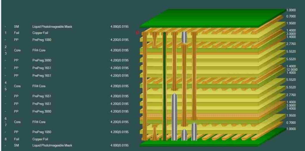
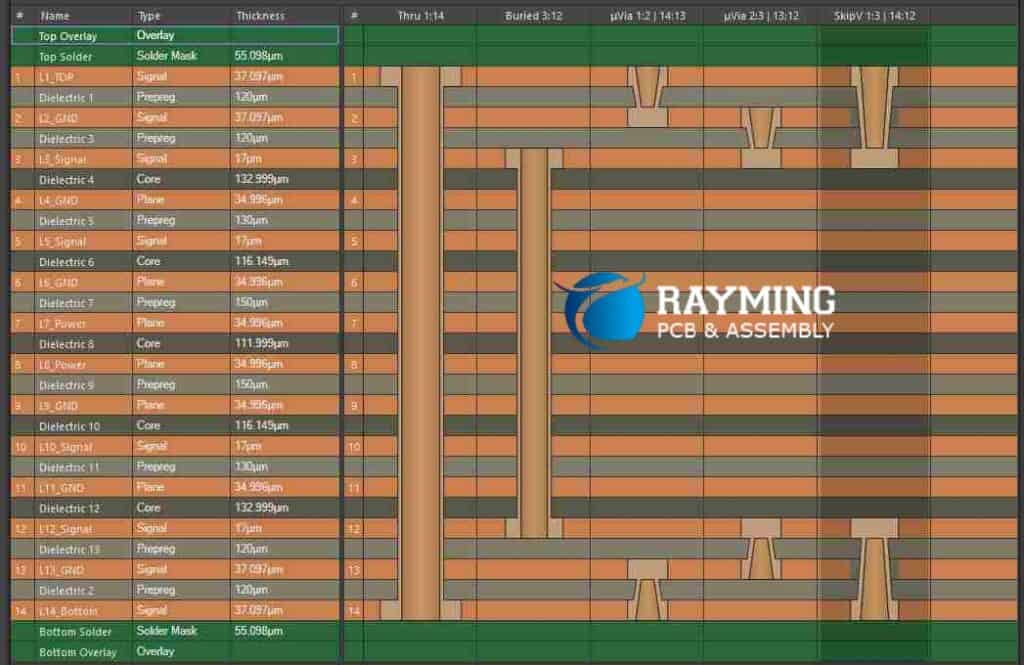
In the ever-evolving world of electronics, the demand for compact and high-performance devices has driven the need for high-density printed circuit boards (PCBs). These specialized PCBs are designed to accommodate a large number of components within a limited space, enabling the development of smaller, more powerful, and more efficient electronic systems. High-density PCBs have become increasingly prevalent in various industries, including consumer electronics, telecommunications, aerospace, and medical equipment.
Understanding PCB Density
Before delving into the specifics of high-density PCBs, it’s essential to understand the concept of PCB density. PCB density refers to the number of components and interconnections that can be accommodated per unit area on a PCB. It is typically measured in components per square inch (cpi) or interconnects per square inch (ipi).
The density of a PCB is influenced by several factors, including:
- Component Size: As component sizes decrease, more components can be placed within a given area, increasing the overall density of the PCB.
- Trace Width and Spacing: Narrower traces and tighter spacing between them allow for more interconnections per unit area, contributing to higher density.
- Via Diameter and Pitch: Smaller via diameters and tighter via pitches enable more vias to be accommodated within a given area, further increasing PCB density.
- Layer Count: PCBs with a higher number of layers can accommodate more interconnections and components, resulting in higher density.
High-density PCBs are designed to maximize the utilization of available board space by optimizing these factors and employing advanced manufacturing techniques.
Characteristics of High-Density PCBs

High-density PCBs exhibit several distinct characteristics that set them apart from conventional PCBs:
1. Increased Component Density
The most defining characteristic of high-density PCBs is their ability to accommodate a significantly higher number of components per unit area compared to standard PCBs. This high component density is achieved through the use of smaller components, finer trace widths and spacing, and advanced manufacturing processes.
2. Smaller Form Factors
Due to the increased component density, high-density PCBs can achieve the same functionality as their larger counterparts while occupying a much smaller physical space. This reduction in form factor is crucial for compact and space-constrained applications, such as mobile devices, wearable electronics, and miniaturized medical equipment.
3. Higher Layer Count
High-density PCBs often feature a higher number of layers compared to standard PCBs. These additional layers provide more routing channels for interconnections, enabling higher component density and more complex circuit designs. Typical high-density PCBs can range from 6 to 24 layers or more.
4. Finer Trace Widths and Spacing
To accommodate more interconnections within a limited area, high-density PCBs employ finer trace widths and tighter trace spacing. These dimensions can range from 3 mil (0.076 mm) trace widths and 3 mil (0.076 mm) spacing down to submicron levels in advanced designs.
5. Smaller Via Diameters and Pitches
High-density PCBs also feature smaller via diameters and tighter via pitches (the distance between adjacent vias). This allows for more vias to be incorporated within the same area, facilitating higher component density and interconnectivity.
6. Advanced Manufacturing Techniques
The production of high-density PCBs requires advanced manufacturing techniques, such as laser drilling, advanced plating processes, and precise imaging and etching methods. These techniques ensure the accurate and reliable fabrication of the intricate features and interconnections found in high-density PCBs.
Applications of High-Density PCBs
High-density PCBs are essential in a wide range of applications where miniaturization, high performance, and compact form factors are critical requirements. Some key applications include:
- Mobile Devices: Smartphones, tablets, and wearable electronics rely heavily on high-density PCBs to pack a multitude of components and functionalities into compact designs.
- Telecommunications Equipment: High-speed data communication systems, such as routers, switches, and base stations, utilize high-density PCBs to accommodate complex circuitry and high-frequency components.
- Aerospace and Defense Systems: Avionics, satellites, and other aerospace systems require high-density PCBs to achieve high performance and reliability while minimizing weight and space requirements.
- Medical Devices: Implantable medical devices, diagnostic equipment, and surgical instruments often employ high-density PCBs to enable miniaturization and advanced functionalities.
- Internet of Things (IoT) Devices: IoT devices, such as sensors, wearables, and smart home appliances, benefit from the compact form factors and high component densities offered by high-density PCBs.
- Automotive Electronics: Advanced driver-assistance systems (ADAS), infotainment systems, and other automotive electronics rely on high-density PCBs to integrate multiple functionalities into limited spaces.
Challenges and Considerations
While high-density PCBs offer numerous advantages, their design and manufacturing also present several challenges and considerations:
- Signal Integrity: With narrower traces, tighter spacing, and higher component densities, maintaining signal integrity becomes a significant challenge. Proper design techniques, such as controlled impedance routing and careful layout planning, are crucial to mitigate signal degradation and electromagnetic interference (EMI) issues.
- Thermal Management: The high component density in high-density PCBs can lead to increased heat generation and thermal management challenges. Appropriate thermal design considerations, including dedicated heat sinks, thermal vias, and efficient airflow, are essential to ensure reliable operation and prevent component failures.
- Manufacturing Complexity: The production of high-density PCBs requires specialized equipment, advanced manufacturing processes, and stringent quality control measures. This complexity can lead to higher manufacturing costs and longer lead times compared to standard PCBs.
- Design Complexity: Designing high-density PCBs involves intricate routing, careful component placement, and meticulous layout planning to ensure signal integrity, thermal management, and manufacturability. Advanced design tools and experienced PCB designers are essential for successful high-density PCB design.
- Testing and Inspection: Due to the compact nature and intricate features of high-density PCBs, testing and inspection processes become more challenging. Advanced techniques, such as automated optical inspection (AOI) and X-ray inspection, may be required to ensure quality and reliability.
- Rework and Repair: Reworking or repairing high-density PCBs can be more difficult and time-consuming due to the small component sizes, tight pitches, and dense interconnections. Specialized tools and techniques may be required for successful rework and repair operations.
Comparison: High-Density PCBs vs. Standard PCBs

To better understand the differences between high-density PCBs and standard PCBs, the following table provides a comparative overview:
| Characteristic | High-Density PCBs | Standard PCBs |
|---|---|---|
| Component Density | High (>100 cpi) | Low to moderate (<100 cpi) |
| Form Factor | Compact and miniaturized | Larger form factors |
| Layer Count | High (6-24 layers or more) | Low to moderate (2-8 layers) |
| Trace Widths and Spacing | Fine (3 mil or less) | Wider (5-10 mil) |
| Via Diameters and Pitches | Small (<10 mil) | Larger (>10 mil) |
| Manufacturing Complexity | High | Moderate |
| Signal Integrity Challenges | Significant | Moderate |
| Thermal Management Considerations | Crucial | Moderate |
| Design Complexity | High | Moderate |
| Testing and Inspection Challenges | High | Moderate |
| Rework and Repair Complexity | High | Moderate |
| Cost | Higher | Lower |
FQA (Frequently Asked Questions)
- Q: What is the main advantage of using high-density PCBs? A: The primary advantage of high-density PCBs is their ability to accommodate a significantly higher number of components and interconnections within a limited board area. This enables the development of compact and miniaturized electronic devices with advanced functionalities.
- Q: Are high-density PCBs more expensive to manufacture than standard PCBs? A: Yes, high-density PCBs are generally more expensive to manufacture than standard PCBs. This is due to the increased complexity of design, advanced manufacturing processes, specialized equipment, and stringent quality control measures required for high-density PCB production.
- Q: Can high-density PCBs be used in high-power applications? A: While high-density PCBs are primarily designed for miniaturization and high component density, they can be used in high-power applications with proper thermal management considerations. Techniques such as dedicated heat sinks, thermal vias, and efficient airflow are essential to ensure reliable operation and prevent overheating.
- Q: Are high-density PCBs more susceptible to signal integrity issues? A: Yes, due to the finer trace widths, tighter spacing, and higher component density, high-density PCBs are more susceptible to signal integrity issues such as crosstalk, electromagnetic interference (EMI), and signal degradation. Proper design techniques, such as controlled impedance routing and careful layout planning, are crucial to mitigate these issues.
- Q: Can high-density PCBs be reworked or repaired easily? A: Reworking or repairing high-density PCBs can be more challenging and time-consuming compared to standard PCBs. This is due to the small component sizes, tight pitches, and dense interconnections. Specialized tools and techniques may be required for successful rework and repair operations on high-density PCBs.


0 Comments