A fiducial on a printed circuit board (PCB) acts as a precise visual reference marker for guiding assembly and inspection machines. Fiducials help align equipment to match the exact locations and orientations defined in the original PCB design data. This aids manufacturing automation and quality control.
In this comprehensive guide, we’ll explain everything you need to know about PCB fiducials including:
- Fiducial Markings
- Pattern Recognition
- Improving Alignment Accuracy
- Optimizing Placement
- Layer and Net Considerations
- Pad Types and Shapes
- Function in Panelization
- Specifying in Documentation
Properly designing quality fiducials directly improves fabrication and assembly yields for your boards. Let’s jump in!
Fiducial Marking Types
There are two main methods for marking fiducial points on PCB layers:
Copper Pads – Exposed metallic landing marker pads provide high visual contrast on insulation layers making recognition more robust. Different width, shape and arrangements help differentiate multiple fiducials.
Silkscreen Marks – Printing fiducials patterns using insulating silkscreen ink defines recognizable images without requiring etching pads. This saves a process step. Various shapes can assist coding.
Both pad and silkscreen fiducials rely on providing clearly identifiable visual targets. Now let’s see how machine vision locates them.
Fiducial Recognition Via Pattern Matching
Automated optical inspection (AOI) systems deploy sophisticated pattern recognition algorithms to identify fiducial markings on boards compared to an ideal reference template. Steps include:
- Scan PCB area via camera without preadjustment
- Detect potential pattern features meeting thresholds
- Extract distinct characteristics like edges, centroids, polarity
- Mathematically correlate characteristics against templates
- Rank pattern similarities determining closest match
- Map board XY offset and rotation from models
- Adjust machine coordinate system to align tool centerpoint
High recognition rates ensure reliable localization even under suboptimal lighting conditions or component obstructions. This facilitates precision assembly population. Next we’ll explore boosting alignment accuracy further.
Improving Fiducial Recognition Accuracy
Achieving precise pattern matching translates directly into tighter pick-and-place tolerances. Here are techniques to refine recognition fidelity:
- Apply unique fiducial shapes and clustering patterns per board region rather than simple repeats
- Frame key groups with asymmetric angular alignments known as Verniers that amplify positional deviations
- Surround critical component fiducials with generous isolation spacing minimizing obstructed visibility
- Designate larger 1.5mm+ pads/features for optical fiducials providing cleaner imagery
- Implement circular polarity markers aiding rotational resolution
- Share reference artworks with manufacturers ensuring optimal template correlations
Every micron of tighter accuracy counts when positioning small chips containing thousands of microscopic leads! Now let’s examine fiducial placement strategies.
Optimizing Fiducial Locations
Equally important as precision lies optimal location across critical board areas:
Component Density – Assign added fiducials near dense sections with many small chips like BGAs requiring precision alignment. More supports improved localization.
Region Distribution – Disperse patterns evenly across left/right and top/bottom quadrants to establish evenly distributed coordinate references including at periphery edges.
One Fiducial Per Region – Align at minimum one recognizable fiducial adjacent to each differentiated assembly/test region to simplify absolute coordinate computations required when switching between areas.
Outside Keepouts – Avoid overlapping fiducials underneath components or very close to pads risking visibility loss when parts get placed or soldered. Fiducials near edges avoid this.
Symmetry Within Panel – Center fiducials symmetrically for each board instance when panelizing to support fracturing individual boards smoothly after population.
With ideal locations set, next we must factor layer assignments.
Layer Planning Factors
Since fiducials define the assembly origin across the entire PCB stackup, applying these practices avoids issues:
Start On Top Layer Pair – Establish initial board coordinate system on the top side first for simplest access, then align all layers below accordingly.
Match Between Layers – Ensureetch patterns and centroids for vertical layer-to-layer pairs align identically so cavities don’t undermine optical recognition.
Place Past Laminate Boundaries – Allow fiducials to slightly overhang designed PCB dimensions so their exposure remains fixed even if boards shift duringlamination alignments introduce small dimensional deltas across batches.
One Layer At Minimum – Always assign at least one working optical fiducial per board on sturdy core insulation layers to guarantee pattern visibility as backup. Silkscreen-only risks lost references if obscured.
With preparations complete, next we must translate concepts into physical pad implementations.
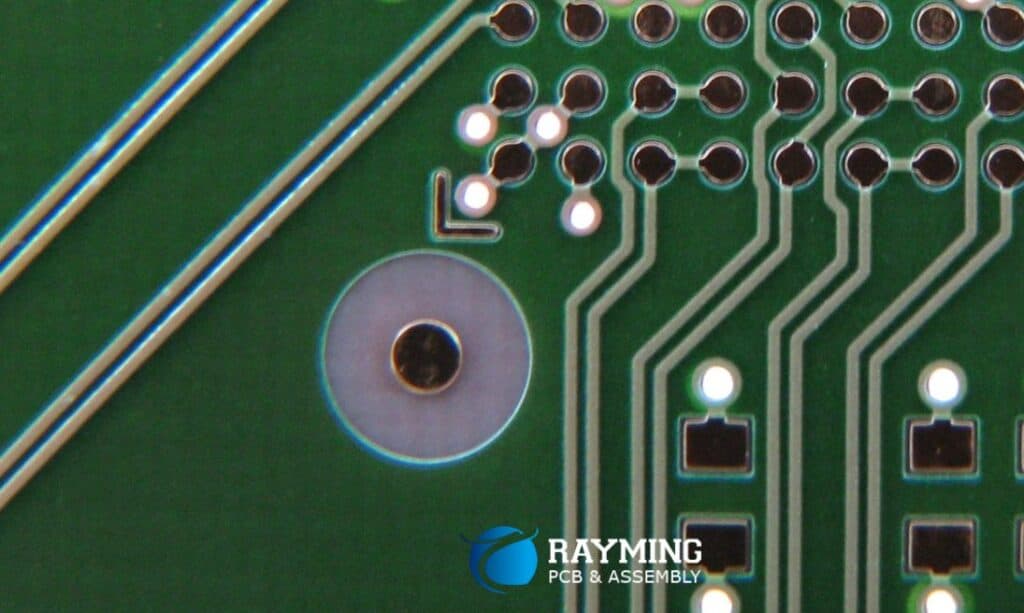
Fiducial Pad Types and Shapes
Besides circular landing pads acting as classic mounts for component leads, fiducial markings leverage an array of specialized patterns:
Crosshairs – Intersecting vertical and horizontal lines or small bars concentrating mass along recognition vectors for precision edge detection.
Concentric Rings – Bullseye-style graduated rings or concentric squares help quantify granular positional deviations during pattern matching providing feedback for precision adjustments.
Alphanumeric Characters – Letters like “FID” help visually identify the marking purpose directly when examining boards.
Asymmetric Shapes – Distinctive irregular patterns, chevrons, polygons or custom images improve detection specificity over basic circles while embedding coded identification data.
In addition to these copper etchings, reference holes as small as 0.3mmSupport tooling alignment applications relying purely on mechanical tip positive pin locations.
Together, such creativeVisible features assist processes for generating, inspecting, assembling and testing boards requiring accurate alignments. As we wrap up, let’s see how fiducials also fit into panelization schemes.
Functionality Within Panelized Boards
Panelization often misaligns individual boards slightly from assumed ideal grid positions. Dedicated fiducials help counteract:
Individual Board Coordinates – Each board contains local fiducials along bottom/left edges establishing its specific internal coordinate system used for positioning components only on that board instance.
Panel-Wide Coordinates – Additional panel-level fiducials placed in empty gutters between boards define global tooling axes for the entire panel to guide automated fabrication, depaneling and handling.
Registration Keys – Interlocking asymmetric circular polarity notches along board boundaries aid perfectly aligning boards for lamination as panels shift between process steps.
Specifying both instance-based and collective panel fiducials supports fracturing finished boards ultimately destined for distinct operational environments depending on final use.
For readers pursuing deeper explorations, numerous illuminating resources exist. But for now, let’s conclude by ensuring fiducial best practices get conveyed downstream properly.
Specifying Fiducials in Design Documentation
While PCB CAD tools provide interactive visual fiducial placement, textually logging key characteristics in detail ensures ideal realization:
Callouts – Annotate locations consolidated on fabrication drawings with centroid coordinates and summary table for quick reference
Dimensions – Numerically quantify nominal diameter and centroid target for each fiducial in callout leaders
Layer Assignments – Denote host layer where applicable to guide stack alignment
Tolerances – Provide maximum acceptable fabrication variance windows if more granular than standard IPC guidelines
References – Cite industry standard templates for pattern matching where relevant along with adjustment methodology specifics per fiducial
Part Numbers – Record part numbers for specialized items like microvia drill targets or optical reference inserts to enable sourcing appropriate articles
Textual specifications help manufacturers align processes with designer expectations for flawless fiducial execution supporting robust volume production.
With that, we conclude our extensive exploration demystifying PCB fiducials! We hope these insights provide a helpful reference next time fiducial functionality becomes relevant in your projects. Let’s wrap by addressing a few common outstanding questions surrounding additional fiducial applications.
Fiducials in PCBs – FAQs
How are fiducials used during board fabrication?
Packing density maximization requires precision layer-to-layer alignment during lamination above 0.1mm tolerances. Embedded tooling holes plus interleaved fiducials guide fine equipment adjustments confirming registration across the stackup.
What inspection use cases involve fiducials?
Various optical metrology and x-ray imaging gear relies on fiducials for calibration. Example applications range from confirming finished hole sizes, quantifying gold finger alloy consistency, measuring RF trace impedances, validating inner layer alignments or profiling via barrel shapes during process audits.
How are fiducials utilized in field repairs?
Field technicians use mounted camera systems that first recognize board fiducials for originating precise coordinate systems guiding component removal, replacement and soldering with tight positional accuracy. This allows automation adaptation.
Can fiducials assist supporting beam-on substrate fabrication?
Yes, scaling future techniques like multi-beam direct-write component assembly requires even tighter real-time optical alignment necessitating easily recognized patterns between layers, so expect fiducials remaining indispensable for next generation electronics fabrication.
While largely invisible elements subtly enhancing manufacturing workflows rather than flashy consumer features, purposefully architected fiducials demonstrate that even the smallest details deserve thoughtfully engineering for optimizing large scale production success. Hopefully this overview better equips your future PCB design fiducial foundations – best wishes pursuing mastery!


0 Comments