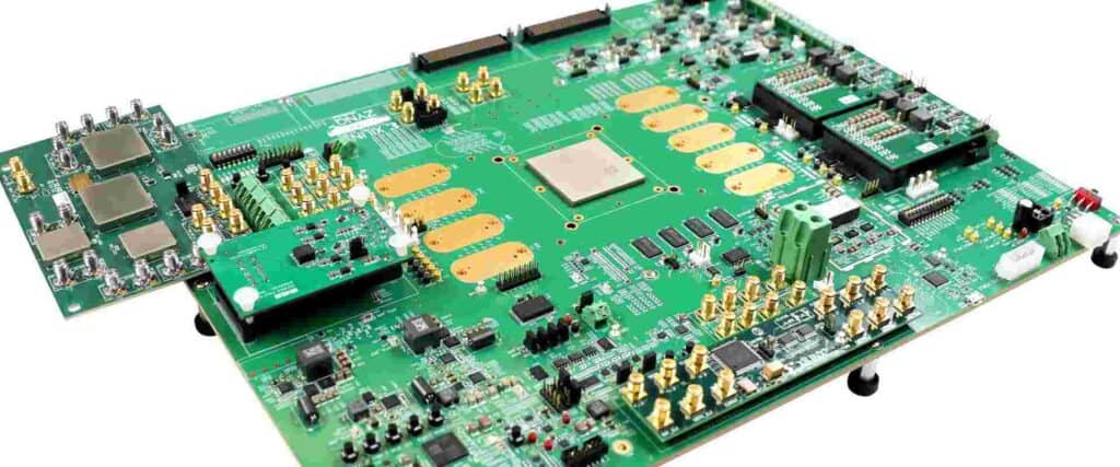
Introduction to Custom PCB Assembly
Printed circuit boards (PCBs) are essential components in nearly all modern electronic devices. A PCB provides the mechanical structure and electrical connections between components in an electronic circuit. While some simple circuits can be constructed on generic PCBs, most electronic products require a custom designed PCB tailored to the specific application.
Custom PCB assembly refers to the process of manufacturing a PCB according to a customer’s unique design requirements. This involves translating the circuit schematic into a physical board layout, selecting PCB fabrication materials, and then assembling the various components onto the board.
Proper PCB assembly is crucial for creating electronic devices that are compact, robust, and high-performing. In this guide, we will explore the key steps, considerations, and benefits of utilizing custom PCB assembly services.
Overview of the PCB Assembly Process
The custom PCB assembly process can be divided into three main phases:
1. Design
The assembly process starts with the schematic capture and PCB layout design. This involves circuit simulation, board layout, routing, and design rule checks. Specialized CAD software is used to translate the logical circuit into an optimized physical form factor for fabrication.
2. Fabrication
Once the design files are finalized, the board fabrication stage begins. This involves creating the physical PCB layers and substrates. Most fabrication today uses advanced techniques like photolithography to etch copper layers onto insulating boards. Different fabrication standards support various complexity needs.
3. Assembly
The last stage is to assemble and solder the components onto the fabricated PCB. This is done using automated pick-and-place machines and soldering systems. The board then undergoes testing and inspection before shipping.
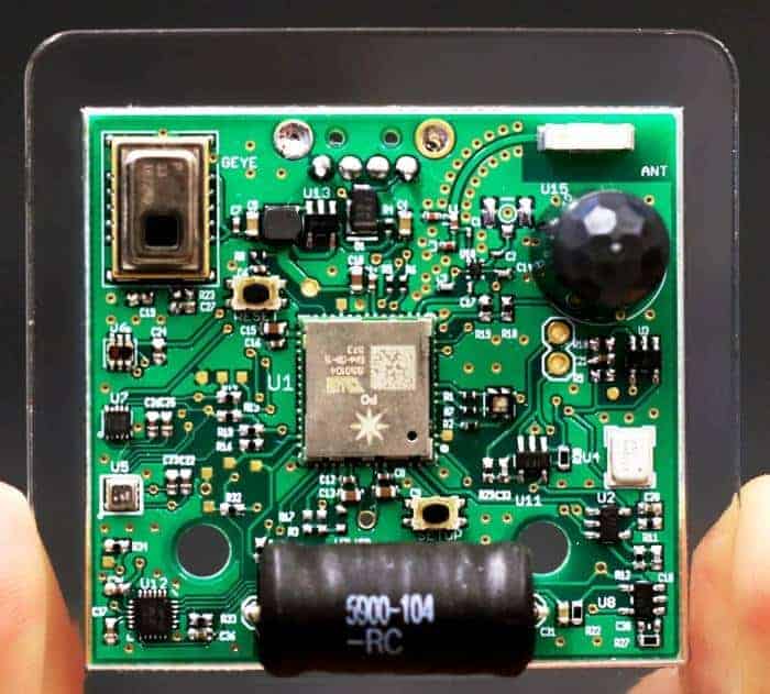
Key Benefits of Custom PCB Assembly
Utilizing custom PCB assembly services offers important benefits compared to alternatives like breadboarding or homemade PCBs:
- Reliability – Professionally assembled PCBs are engineered to withstand mechanical and electrical stresses. Rigorous testing procedures verify robust operation.
- Miniaturization – Careful component placement and routing allows for extreme space optimization and weight reduction.
- Reproducibility – Consistent quality and performance are ensured by standardized assembly procedures. Large production volumes are feasible.
- Efficiency – Automated assembly systems are much faster and cheaper compared to manual assembly or prototyping.
- Support – Experienced assembly partners provide end-to-end support, from design review to manufacturing consulting.
PCB Assembly Process Step-by-Step
Now let’s take a closer look at the typical workflow for custom PCB assembly:
1. Design and Layout
- Create schematics for each functional block using CAD tools like OrCAD, Altium, Eagle, etc. Perform circuit simulation.
- Translate schematics into board layout. Place components and route connections on 2D layout canvas.
- Run design rule checks to verify trace widths, clearances, etc.
- Add text annotations, fabrication notes, solder masks, and silkscreens.
- Export Gerber, drill, and assembly files. Share with assembly partner.
2. Prototyping
- Build prototype boards in small batches to test functionality.
- Use barebones assembly services without solder masks or silkscreens to save cost.
- Identify any needed design modifications from prototypes.
- Repeat prototyping until design is finalized.
3. Fabrication
- Choose PCB substrate material (FR-4, polyimide, ceramic, etc.). Evaluate board thickness.
- Select number of conductive layers (2 to 32+). More layers allow greater routing density.
- Determine copper thickness, typically 1-2 oz for outer layers and 0.5-1 oz for inner layers.
- Define minimum trace/space based on circuit complexity. Today’s limit is ~5/5 mil (0.127mm).
- Specify hole sizes and tolerances. For 2:1 aspect ratio, min. hole is 8mil (0.2mm).
- Identify board edge treatments like V-scoring, routing, etc.
- Submit Gerber files to board fabrication plant and order boards.
4. Assembly
- Plan component placement to minimize wire lengths and heating.
- Group components into SMD (surface-mount) and through-hole types.
- Apply solder paste on pads for SMD components. Use solder masks to control application.
- Use pick-and-place machines to accurately position components on boards.
- For through-hole parts, insert leads/pins manually or by machine.
- Use wave soldering system or reflow oven to form solder joints.
- Clean boards and inspect solder joints under microscope. Re-work any issues.
- Test board operation with electrical validation and functional testing.
5. Box Build
- Add any auxiliary hardware like connectors, cables, chassis, etc.
- Configure and load any firmware or software elements.
- Perform complete system-level test on finished product.
- Quality checks and final certification for shipping to customer.
Choosing the Right PCB Assembly Partner
Choosing an experienced, high-quality PCB assembly company is crucial for avoiding expensive re-works and ensuring properly functioning products. Here are some key factors to evaluate potential assembly partners on:
| Consideration | Importance |
|---|---|
| Technology | Advanced SMT lines, automated assembly/test |
| Quality | IPC certifications, rigorous testing |
| Volume capacity | Scalable from small batches to mass production |
| Design support | DFM analysis and engineering reviews |
| Lead time | Fast turnaround options |
| Supply chain management | Vast component inventory and sourcing |
| Cost | Competitive pricing, NRE discounts |
| Communication | Technical expertise and customer service |
Mistakes to Avoid in PCB Assembly
Here are some common mistakes to avoid when designing boards destined for professional assembly:
- Insufficient component clearance – Leave adequate spacing around parts for soldering and rework.
- Impossible to assemble parts – Avoid tiny 01005 passives and large BGAs with tight pitches.
- Inconsistent symbol libraries – Use a unified library to avoid mismatched footprints.
- Un-solderable traces – Minimum trace width is ~8 mil (0.2mm) or >10-20mil for hand-soldering.
- Excessive component counts – Hundreds of unique parts will drive up assembly time and cost. Consolidate where possible.
- Odd board shapes – Stick to rectangular PCBs instead of circular or very irregular shapes.
- No test points – Include test pads connected to nets/traces so voltages can be probed.
- Lack of instructions – Clearly specify any critical assembly/soldering sequences or concerns.
Conclusion
Custom PCB assembly enables creating electronic products with optimized performance, reliability, and manufacturability. By partnering with a full-service assembly provider, companies can introduce new designs faster and scale up production rapidly. With careful planning and upfront design-for-assembly analysis, it’s possible to develop even highly complex PCBs affordably and efficiently through custom assembly processes. The result is high-quality electronic products that meet demanding mechanical, electrical, and business objectives.
Frequently Asked Questions
Q1: What are the most common PCB substrate materials?
The most popular PCB substrate is FR-4 fiberglass, which offers good mechanical strength and temperature resistance. Other common options include CEM-1/3 cotton paper, Rogers high-frequency boards, polyimide, and aluminum or steel metal core boards.
Q2: What is HAL lead-free soldering?
HAL (Hot Air Leveled) soldering uses hot air jets to flatten molten lead-free solder after SMT component placement. This improves joint coplanarity. Lead-free solders like SAC305 (Sn/Ag/Cu) are environmentally safer but harder to work with than traditional leaded solders.
Q3: What is the function of a solder mask?
A solder mask is a coated layer that controls solder application on PCBs. The mask blocks solder from depositing in unwanted areas, preventing bridging shorts. Common solder mask colors are green, red, yellow, blue, black, and white.
Q4: How are PCB hole sizes specified?
PCB holes use imperial units in mils or millimeters. Hole diameters are specified relative to the drill bit size. For example, common sizes are 0.020″ (20mil), 0.031″ (31mil), 0.062″ (62mil), etc. Tighter hole tolerances allow smaller via sizes.
Q5: What is the most important design rule for assembly?
Sufficient clearance space around pads and components is the most critical rule. This guarantees adequate room for solder application and reworking during assembly. IPC-7351B recommends 8mil clearance for SMT pads, and 16mil to 20mil for through-hole parts.


0 Comments