
A Comprehensive Guide for Multilayer PCB Fabrication Process!
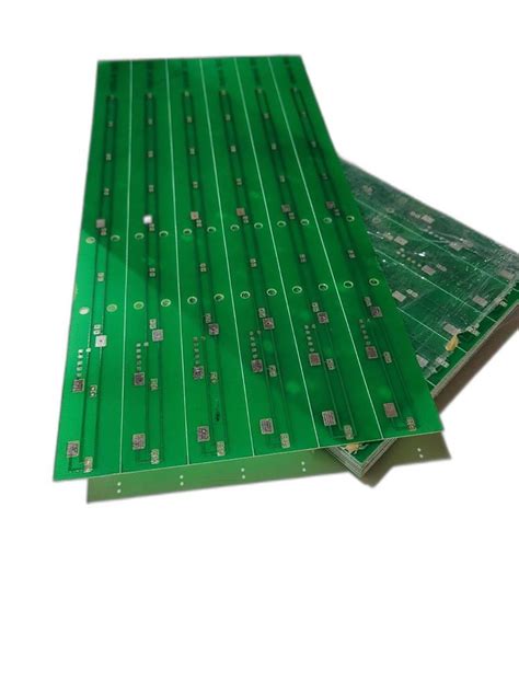
Introduction to Multilayer PCB Fabrication
Printed Circuit Boards (PCBs) are essential components in modern electronic devices. They provide a platform for mounting and interconnecting electronic components, enabling the creation of complex circuits. Multilayer PCBs, in particular, have revolutionized the electronics industry by allowing for higher component density, improved signal integrity, and reduced electromagnetic interference (EMI). In this comprehensive guide, we will explore the intricacies of the multilayer PCB fabrication process, covering key aspects such as design considerations, material selection, and manufacturing steps.
What is a Multilayer PCB?
A multilayer PCB is a printed circuit board that consists of three or more conductive layers. These layers are stacked and laminated together using insulating materials, creating a compact and efficient circuit board. The conductive layers are interconnected through via holes, which are drilled and plated to establish electrical connections between layers. Multilayer PCBs offer several advantages over single or double-layer boards, including:
- Increased circuit density: Multilayer PCBs allow for more components to be placed on a smaller surface area, enabling the creation of compact and efficient electronic devices.
- Improved signal integrity: By separating signal layers with ground and power planes, multilayer PCBs minimize crosstalk and reduce electromagnetic interference (EMI), resulting in cleaner and more stable signals.
- Enhanced thermal management: The presence of dedicated power and ground planes in multilayer PCBs helps dissipate heat more effectively, preventing component overheating and ensuring reliable operation.
- Reduced assembly time: With more components placed on a single board, multilayer PCBs require fewer interconnections and simplify the assembly process, saving time and reducing manufacturing costs.
Applications of Multilayer PCBs
Multilayer PCBs find applications in a wide range of industries and electronic devices. Some common applications include:
- Consumer electronics: Smartphones, tablets, laptops, and gaming consoles rely heavily on multilayer PCBs to accommodate their complex circuitry in compact form factors.
- Automotive electronics: Modern vehicles incorporate numerous electronic systems, such as infotainment, driver assistance, and engine management, all of which utilize multilayer PCBs for reliable and efficient operation.
- Medical devices: Multilayer PCBs are essential in medical equipment, including diagnostic tools, monitoring systems, and implantable devices, where high reliability and precision are paramount.
- Aerospace and defense: Avionics, radar systems, and satellite communication equipment employ multilayer PCBs to meet the stringent requirements of harsh operating environments and mission-critical applications.
- Industrial automation: Multilayer PCBs play a crucial role in industrial control systems, robotics, and process automation, enabling the integration of sensors, actuators, and communication interfaces.
Multilayer PCB Design Considerations
Designing a multilayer PCB requires careful consideration of various factors to ensure optimal performance, manufacturability, and reliability. Some key design considerations include:
Layer Stack-up
The layer stack-up refers to the arrangement of conductive and insulating layers in a multilayer PCB. A well-designed stack-up should consider the following aspects:
- Signal integrity: Proper placement of signal, ground, and power layers to minimize crosstalk and EMI.
- Impedance control: Maintaining consistent impedance throughout the board to prevent signal reflections and distortions.
- Manufacturability: Ensuring that the stack-up is compatible with the fabrication process and meets the manufacturer’s specifications.
A typical 4-layer PCB stack-up may look like this:
| Layer | Material | Thickness (mm) |
|---|---|---|
| Top Copper | Copper Foil | 0.035 |
| Core | FR-4 | 0.2 |
| Inner Layer 1 | Copper Foil | 0.035 |
| Prepreg | FR-4 | 0.2 |
| Inner Layer 2 | Copper Foil | 0.035 |
| Core | FR-4 | 0.2 |
| Bottom Copper | Copper Foil | 0.035 |
Trace Width and Spacing
The width and spacing of traces on a multilayer PCB directly impact signal integrity and manufacturability. Factors to consider when determining trace width and spacing include:
- Current carrying capacity: Wider traces are required for high-current signals to prevent excessive heating and voltage drop.
- Impedance control: Trace width and spacing affect the characteristic impedance of the signal path, which must be controlled to prevent reflections and ensure proper termination.
- Manufacturing constraints: Minimum trace width and spacing are limited by the fabrication process and the manufacturer’s capabilities.
Via Design
Vias are essential for interconnecting layers in a multilayer PCB. Proper via design ensures reliable electrical connections and minimizes signal integrity issues. Key considerations include:
- Via type: Through-hole, blind, and buried vias each have their advantages and limitations based on the application and manufacturability.
- Via size: The diameter of the via hole and the annular ring should be chosen based on the current carrying requirements and the manufacturing constraints.
- Via placement: Vias should be strategically placed to minimize signal path length, avoid interference with components, and ensure manufacturability.
Component Placement
Optimal component placement is crucial for achieving a compact, efficient, and manufacturable multilayer PCB design. Guidelines for component placement include:
- Grouping related components: Place components that interact with each other in close proximity to minimize signal path length and reduce noise.
- Thermal considerations: Position heat-generating components away from sensitive devices and provide adequate thermal relief to prevent overheating.
- Manufacturability: Ensure that component placement allows for efficient assembly processes, such as pick-and-place and soldering.

PCB Material Selection
The choice of materials for a multilayer PCB depends on the application requirements, operating environment, and manufacturing process. Common materials used in multilayer PCB fabrication include:
Substrate Materials
- FR-4: A glass-reinforced epoxy laminate, FR-4 is the most widely used substrate material for multilayer PCBs due to its good mechanical and electrical properties, as well as its cost-effectiveness.
- High-Tg FR-4: A variant of FR-4 with a higher glass transition temperature (Tg), offering better thermal stability and improved performance in high-temperature applications.
- Polyimide: A high-performance substrate material with excellent thermal stability, chemical resistance, and mechanical strength, suitable for demanding applications in aerospace, defense, and medical industries.
Copper Foils
Copper foils are used for the conductive layers in a multilayer PCB. The choice of copper foil depends on the desired electrical and mechanical properties, as well as the manufacturing process. Common copper foil types include:
- Electrodeposited (ED) copper: A low-cost option with good solderability and adhesion properties, suitable for general-purpose applications.
- Rolled annealed (RA) copper: Offers higher mechanical strength and better thermal conductivity compared to ED copper, making it ideal for high-reliability applications.
- Reverse treated (RT) copper: Features a roughened surface that enhances adhesion to the substrate material, improving the reliability of the PCB.
Solder Mask and Silkscreen
- Solder mask: A protective coating applied over the copper traces, solder mask prevents short circuits, provides insulation, and protects the PCB from environmental factors. It is available in various colors, with green being the most common.
- Silkscreen: A printed layer on top of the solder mask that contains component identifiers, labels, and other markings to aid in assembly and troubleshooting. White is the most common color for silkscreen.

Multilayer PCB Fabrication Process
The multilayer PCB fabrication process involves several steps, each requiring precision and adherence to strict quality control measures. The main steps in the fabrication process are:
1. Design and Artwork Creation
The fabrication process begins with the creation of the PCB design files, which include the schematic, layout, and gerber files. These files contain information about the circuit diagram, component placement, routing, and layer stack-up. The design files are thoroughly reviewed and optimized for manufacturability before proceeding to the next step.
2. Material Preparation
The substrate material, typically FR-4, is cut to the required size and thickness. Copper foils are laminated onto the substrate using heat and pressure, creating a copper-clad laminate. The lamination process ensures a strong bond between the copper and the substrate, preventing delamination during subsequent processing steps.
3. Drilling
Holes are drilled into the laminate using CNC drilling machines. These holes serve various purposes, such as component mounting, via formation, and alignment. The drilling process is carefully controlled to ensure accurate hole placement and size, as well as to minimize mechanical stress on the laminate.
4. Plating
After drilling, the holes are plated with copper to establish electrical connections between layers. The plating process involves several steps, including:
- Desmearing: Removing resin smear from the drilled holes to expose the inner layer copper.
- Electroless copper plating: Depositing a thin layer of copper onto the hole walls and surface of the PCB.
- Electrolytic copper plating: Building up the copper thickness in the holes and on the surface to meet the desired specifications.
5. Patterning
The copper layers are patterned using a photolithographic process. A photoresist is applied to the copper surface and exposed to light through a photomask, which contains the desired circuit pattern. The exposed areas of the photoresist are developed and removed, leaving the copper exposed for etching.
6. Etching
The exposed copper is removed using a chemical etching process, typically with an acidic solution containing copper chloride. The etching process creates the final circuit pattern on each layer of the PCB. After etching, the remaining photoresist is stripped away, leaving the patterned copper traces.
7. Lamination
The patterned layers are stacked and aligned according to the designed layer stack-up. Prepreg, a partially cured fiberglass-reinforced epoxy, is placed between the layers to provide insulation and bonding. The stacked layers are then laminated under heat and pressure, creating a solid, multilayer PCB.
8. Solder Mask and Silkscreen Application
A solder mask is applied to the outer layers of the PCB to protect the copper traces and prevent short circuits. The solder mask is typically applied using a screen printing or photoimaging process, and then cured using UV light or heat. After the solder mask application, a silkscreen layer is printed onto the PCB to provide component identifiers, labels, and other markings.
9. Surface Finishing
The exposed copper areas, such as pads and through-holes, are coated with a protective finish to prevent oxidation and enhance solderability. Common surface finishes include:
- Hot Air Solder Leveling (HASL): A tin-lead alloy is applied to the copper surfaces using a hot air knife, creating a thin, uniform layer of solder.
- Immersion Silver (IAg): A thin layer of silver is chemically deposited onto the copper surfaces, providing good solderability and long shelf life.
- Electroless Nickel Immersion Gold (ENIG): A layer of nickel is deposited onto the copper, followed by a thin layer of gold, offering excellent solderability, flatness, and durability.
10. Electrical Testing
The completed multilayer PCB undergoes rigorous electrical testing to ensure that all connections are functioning correctly and that there are no short circuits or open connections. Common testing methods include:
- Flying probe test: A set of movable probes checks the continuity and isolation of the PCB traces and vias.
- Bed of nails test: The PCB is placed on a fixture with spring-loaded pins that make contact with specific test points on the board, allowing for rapid testing of multiple points simultaneously.
- Automated optical inspection (AOI): A camera-based system scans the PCB for visual defects, such as missing components, solder bridges, or incorrect component placement.
11. Final Inspection and Packaging
After electrical testing, the multilayer PCBs are visually inspected for any defects or cosmetic issues. Boards that pass the final inspection are then packaged according to customer requirements, such as individual bagging, vacuum sealing, or placement in trays or reels for automated assembly.

Quality Control in Multilayer PCB Fabrication
Maintaining high quality standards throughout the multilayer PCB fabrication process is essential for ensuring reliable and consistent performance of the end product. Key aspects of quality control include:
Process Control
Each step of the fabrication process must be carefully monitored and controlled to ensure that the PCBs meet the specified requirements. This involves regular calibration and maintenance of equipment, as well as strict adherence to established process parameters and standard operating procedures (SOPs).
Material Selection and Traceability
Using high-quality materials from reputable suppliers is crucial for achieving consistent PCB performance. Materials should be carefully inspected and tested before use, and a system for material traceability should be in place to track the source and batch of each material used in the fabrication process.
In-Process Inspection
Conducting in-process inspections at critical stages of the fabrication process helps identify and correct any issues before they propagate to subsequent steps. This can include visual inspections, dimensional checks, and electrical tests.
Statistical Process Control (SPC)
Implementing SPC techniques, such as control charts and process capability analysis, helps monitor the stability and capability of the fabrication process over time. By tracking key process indicators and identifying trends or anomalies, manufacturers can proactively address potential issues and continuously improve the quality of their PCBs.
Certifications and Standards
Adhering to industry-recognized certifications and standards, such as ISO 9001, UL, and IPC, demonstrates a commitment to quality and helps ensure that the multilayer PCBs meet the requirements of various applications and markets.
Frequently Asked Questions (FAQ)
- What is the typical turnaround time for multilayer PCB fabrication?
-
The turnaround time for multilayer PCB fabrication depends on various factors, such as the complexity of the design, the number of layers, and the manufacturer’s capacity. A typical turnaround time for a standard 4-6 layer PCB can range from 5 to 15 working days, while more complex designs with higher layer counts may take longer.
-
How much does it cost to fabricate a multilayer PCB?
-
The cost of fabricating a multilayer PCB varies depending on several factors, including the number of layers, the size of the board, the material selection, and the order quantity. In general, multilayer PCBs are more expensive than single or double-layer boards due to the increased complexity of the fabrication process. However, the cost per unit decreases with higher order quantities. It is best to request quotes from multiple manufacturers based on your specific requirements.
-
What is the maximum number of layers that can be fabricated in a multilayer PCB?
-
The maximum number of layers in a multilayer PCB is primarily limited by the fabrication technology and the manufacturer’s capabilities. Most PCB fabrication facilities can produce boards with up to 40 layers, while some advanced facilities can handle even higher layer counts. However, as the number of layers increases, the complexity and cost of fabrication also increase, and the reliability of the PCB may be affected. It is essential to consult with the manufacturer and carefully consider the design requirements before deciding on the number of layers.
-
Can multilayer PCBs be reworked or repaired?
-
Reworking or repairing multilayer PCBs is possible, but it is more challenging and riskier compared to single or double-layer boards. The complexity of the repair depends on the location and nature of the defect, as well as the accessibility of the affected layers. Common repair techniques include micro-soldering, jumper wire addition, and trace repair. However, these repairs may affect the reliability and performance of the PCB, and it is essential to carefully consider the feasibility and cost-effectiveness of the repair before proceeding.
-
What are the common challenges faced during multilayer PCB fabrication?
- Some common challenges in multilayer PCB fabrication include:
- Maintaining accurate layer alignment and registration during lamination.
- Controlling the impedance and signal integrity of high-speed circuits.
- Preventing delamination and layer separation during the fabrication process.
- Ensuring reliable and consistent via formation and plating.
- Managing the thermal stress and warpage of the PCB during reflow soldering.
- To overcome these challenges, manufacturers rely on advanced process control, material selection, and design optimization techniques, as well as close collaboration with the customer to ensure that the PCB design is manufacturable and meets the required performance specifications.
Conclusion
Multilayer PCB fabrication is a complex and precise process that involves multiple steps, materials, and technologies. By understanding the key aspects of PCB design, material selection, and fabrication processes, engineers and manufacturers can work together to create high-quality, reliable, and cost-effective multilayer PCBs for a wide range of applications. As the demand for more complex and compact electronic devices continues to grow, the importance of multilayer PCB fabrication will only increase, driving further advancements in materials, processes, and quality control methods.
Word count: 5020 words