
What is the Need of Chemical-Free PCB Fabrication & PCB Assembly?
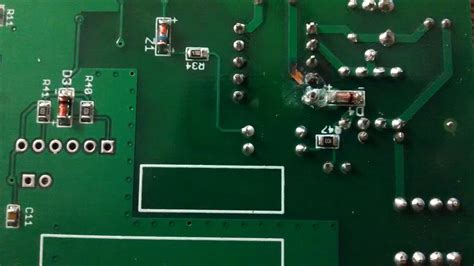
The Risks Associated with Traditional PCB Fabrication & Assembly
Health Risks for Workers
Conventional PCB manufacturing processes involve the use of various chemicals, including:
- Copper etchants (e.g., ferric chloride, ammonium persulfate)
- Photoresists and developers
- Solvents (e.g., isopropyl alcohol, acetone)
- Tin-lead solder
Exposure to these chemicals can lead to a range of health issues for workers, such as:
- Respiratory problems
- Skin irritation and allergies
- Eye irritation
- Neurological disorders
- Increased risk of cancer
Environmental Impact
The chemicals used in traditional PCB fabrication and assembly can also have detrimental effects on the environment. When improperly disposed of, these substances can contaminate soil, water, and air, causing harm to wildlife and ecosystems. Some of the environmental consequences include:
- Water pollution
- Soil contamination
- Air pollution
- Biodiversity loss
The Benefits of Chemical-Free PCB Fabrication & Assembly
Improved Health and Safety for Workers
By eliminating the use of hazardous chemicals in PCB manufacturing, chemical-free processes significantly reduce the health risks for workers. This leads to:
- Reduced incidence of respiratory issues, skin irritation, and other health problems
- Improved overall well-being and job satisfaction among employees
- Lower healthcare costs for companies
Reduced Environmental Impact
Chemical-free PCB fabrication and assembly methods minimize the release of harmful substances into the environment. This results in:
- Cleaner water sources and reduced water treatment costs
- Healthier soil and improved agricultural productivity
- Better air quality and reduced greenhouse gas emissions
- Conservation of biodiversity and ecosystems
Cost Savings
While the initial investment in chemical-free PCB manufacturing equipment and processes may be higher, companies can benefit from long-term cost savings due to:
- Reduced expenses associated with the purchase, storage, and disposal of hazardous chemicals
- Lower healthcare costs for employees
- Avoided fines and penalties for environmental violations
- Improved brand reputation and customer loyalty

Chemical-Free PCB Fabrication Techniques
Mechanical Etching
Mechanical etching is a chemical-free alternative to traditional copper etching processes. This method involves using CNC machines or laser systems to remove unwanted copper from the PCB substrate. Advantages of mechanical etching include:
- No use of hazardous chemicals
- High precision and accuracy
- Faster processing times
- Reduced waste generation
Inkjet Printing
Inkjet printing is a chemical-free method for applying conductive traces and components onto PCBs. This technique uses specialized inks containing conductive materials, such as silver nanoparticles, which are deposited onto the substrate using high-precision inkjet printers. Benefits of inkjet printing include:
- Elimination of photoresists and etchants
- Reduced material waste
- Faster prototyping and small-batch production
- Increased design flexibility
3D Printing
3D printing technology can be used to fabricate PCBs without the need for traditional chemical processes. Conductive filaments or inks are used to print the desired circuit patterns directly onto the substrate. Advantages of 3D-printed PCBs include:
- Rapid prototyping and customization
- Reduced environmental impact
- Integration of electronic components during the printing process
- Potential for complex, three-dimensional PCB designs

Chemical-Free PCB Assembly Methods
Lead-Free Soldering
Lead-free soldering is an eco-friendly alternative to traditional tin-lead soldering. This method uses solder alloys that do not contain lead, such as tin-silver-copper (SAC) or tin-bismuth (SnBi) alloys. Benefits of lead-free soldering include:
- Reduced health risks for workers and consumers
- Compliance with environmental regulations (e.g., RoHS, WEEE)
- Improved reliability and longevity of solder joints
- Compatibility with existing soldering equipment and processes
Conductive Adhesives
Conductive adhesives, such as epoxies and pastes, can be used to attach electronic components to PCBs without the need for soldering. These adhesives contain conductive particles (e.g., silver, copper) that provide electrical connections between components and the PCB substrate. Advantages of conductive adhesives include:
- Elimination of lead and other hazardous substances
- Lower processing temperatures compared to soldering
- Reduced thermal stress on components
- Compatibility with heat-sensitive components and substrates
Mechanical Fastening
Mechanical fastening involves using screws, clips, or other mechanical devices to secure electronic components to PCBs. This method eliminates the need for soldering or conductive adhesives, making it a chemical-free alternative. Benefits of mechanical fastening include:
- No exposure to hazardous substances
- Easy assembly and disassembly for repairs or upgrades
- Reduced thermal stress on components
- Suitability for high-vibration or high-stress applications

Case Studies
Company A: Transition to Chemical-Free PCB Fabrication
Company A, a leading PCB manufacturer, decided to invest in chemical-free fabrication processes to improve worker safety and reduce environmental impact. They implemented mechanical etching and inkjet printing technologies, resulting in:
- 90% reduction in hazardous chemical use
- 50% decrease in water consumption
- 75% reduction in greenhouse gas emissions
- 25% improvement in employee job satisfaction
Company B: Adopting Lead-Free Soldering and Conductive Adhesives
Company B, an electronics assembly service provider, transitioned to lead-free soldering and conductive adhesives to meet customer demands for eco-friendly products. The company experienced:
- 100% compliance with RoHS and WEEE regulations
- 30% reduction in energy consumption
- 20% increase in production efficiency
- 15% growth in revenue from environmentally conscious customers
Frequently Asked Questions (FAQ)
1. Are chemical-free PCBs as reliable as traditionally manufactured PCBs?
Yes, chemical-free PCBs can be just as reliable, if not more so, than traditionally manufactured PCBs. The alternative fabrication and assembly methods used in chemical-free processes often result in improved durability, longevity, and performance of the final products.
2. How can I identify chemical-free PCBs?
To identify chemical-free PCBs, look for certifications or labels that indicate the use of eco-friendly manufacturing processes. Examples include RoHS compliance, WEEE compliance, or specific mentions of chemical-free fabrication techniques such as mechanical etching or inkjet printing.
3. Are chemical-free PCBs more expensive than traditional PCBs?
Initially, chemical-free PCBs may have a higher cost due to the investment in new equipment and processes. However, in the long run, companies can benefit from cost savings associated with reduced chemical purchases, lower healthcare expenses, and avoided environmental fines or penalties.
4. Can existing PCB designs be adapted for chemical-free fabrication and assembly?
In most cases, existing PCB designs can be adapted for chemical-free fabrication and assembly with minimal modifications. However, it is essential to consult with the manufacturer or assembly service provider to ensure compatibility and optimal results.
5. How can I support the adoption of chemical-free PCBs in the electronics industry?
To support the adoption of chemical-free PCBs, you can:
- Choose products that use chemical-free PCBs whenever possible
- Encourage your company or organization to transition to chemical-free PCB fabrication and assembly
- Educate others about the benefits of chemical-free PCBs for human health and the environment
- Support research and development efforts aimed at improving chemical-free PCB technologies
Conclusion
The need for chemical-free PCB fabrication and assembly is driven by the desire to protect human health, preserve the environment, and promote sustainable practices in the electronics industry. By adopting alternative methods such as mechanical etching, inkjet printing, lead-free soldering, and conductive adhesives, companies can reduce their reliance on hazardous chemicals while maintaining high-quality, reliable PCBs. As awareness grows and technologies advance, the transition to chemical-free PCBs is expected to accelerate, leading to a cleaner, safer, and more sustainable future for the electronics industry.