Manufacturing
Surface mount technology (SMT) has revolutionized the electronics manufacturing industry over the past few decades. SMT enables the placement of electronic components directly onto the surface of printed circuit boards (PCBs) without the need for through-hole mounting. This has allowed for miniaturization and automation in electronics production. In this comprehensive guide, we will explore the key aspects of modern SMT electronics manufacturing.
Overview of the SMT Assembly Process
The surface mount assembly process can be broken down into three main stages:
SMT Component Placement
During this stage, pick and place machines automatically populate PCBs by rapidly and precisely positioning electronic components based on programmed instructions. Feeders supply a constant stream of components to the pick and place head for placement onto solder paste deposits on the PCB.
SMT Soldering
After component placement, the PCBs pass through industrial soldering ovens which use convection, infrared radiation or vapor phase to melt solder paste deposits, forming reliable electrical and mechanical joints. The solder joints anchor components in place on the board.
Inspection and Testing
Once soldering is complete, automated optical inspection (AOI) machines use high resolution cameras to examine PCBs and identify any assembly defects. Electrical testing equipment also verifies that circuits function as intended.
SMT Components
A wide variety of miniature electronic components are designed for surface mounting, including:
- Resistors and capacitors – Tiny surface mount devices (SMDs) include chip resistors, multi-layer ceramic capacitors (MLCCs), etc.
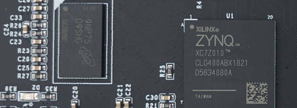
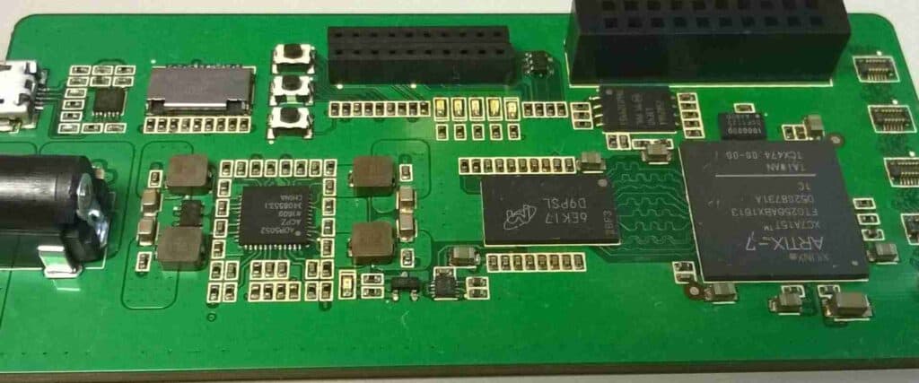
- Integrated circuits (ICs) – This includes application specific ICs (ASICs), microprocessors, memory chips and other ICs in small plastic or ceramic SMT packages.
- Semiconductors – SMT diodes, transistors, and rectifiers.
- Connectors – Low profile board-to-board, board-to-cable, and ribbon cable connectors.
Comparison of Common SMT Component Packages
| Package | Description |
|---|---|
| SOIC (Small Outline IC) | Rectangular plastic body package for ICs |
| QFP (Quad Flat Pack) | Square IC package with leads on all four sides |
| TSOP (Thin Small Outline Package) | Thin rectangular plastic IC package |
| QFN/DFN (Quad/Dual Flat No-lead) | Low profile square IC package with leads underneath |
| 0201, 0402, etc. | Diminishingly small SMD resistor/capacitor sizes |
SMT Equipment and Materials
Automated assembly of surface mount PCBs relies on precise equipment and materials:
SMT Printers
Stencil printers use fine metal stencils to accurately deposit tiny solder paste deposits onto PCB bonding pads, where components will be placed.
Pick and Place Machines
These robotic machines use vacuum nozzles to pick components from feeders and position them onto solder paste on the PCB with extreme accuracy. Advanced systems can place over 100,000 components per hour.
SMT Soldering Equipment
Reflow ovens use temperature profiles to gradually heat solder paste deposits to a liquid state, securing component leads with excellent solder joints.
AOI Machines
Automated optical inspection systems use high resolution cameras to identify any assembly flaws so they can be reworked.
Solder Paste
Solder paste contains solder alloy particles suspended in flux. It prints smoothly through stencils and forms reliable solder joints after reflow.
Advantages of SMT
Here are some of the main benefits that SMT electronics manufacturing provides:
- Miniaturization – By eliminating through-holes, components can be packed more densely on PCBs, enabling smaller and lighter end products.
- Higher Productivity – Automated assembly reduces manufacturing times and increases output volumes.
- Improved Reliability – SMT avoids weaknesses associated with through-hole assembly and can produce very reliable solder joints.
- Lower Costs – Smaller components + automated assembly = reduced manufacturing costs.
- Double-Sided Assembly – SMT allows components to be placed on both sides of PCBs.
SMT Design Considerations
To fully leverage SMT capabilities, engineers should adhere to SMT design principles:
- Use the smallest component sizes that meet electrical requirements.
- Place components with the highest pin count in the center of the board first.
- Group components according to type for easier pick and place programming.
- Allow sufficient clearance between components for soldering.
- Use solder masks to prevent solder bridging between dense conductor traces.
- Include fiducials and other features to facilitate automated assembly.
- Minimize component placements requiring human intervention.
With careful design for manufacturability, products can achieve maximum quality, yield, and cost competitiveness.
Quality Control in SMT Production
Maintaining quality in SMT assembly involves:
- Statistical process control tracking of critical parameters.
- Inspecting and testing of solder paste printing.
- Monitoring pick and place accuracy and efficiency.
- Controlling reflow oven profiles.
- Verifying solder joint integrity and surface finishes.
- AOIs inspecting for assembly issues like missing components.
- Functionally testing PCBs using boundary scan, flying probe or ICT fixtures.
By closely overseeing these processes, defects can be eliminated through continual optimization.
SMT Rework and Repair
When flaws occur, it is preferable to rework PCBs rather than scrap them. Common rework methods include:
- Reflowing solder joints using hot air tools.
- Removing/replacing components using soldering irons, desoldering tools, etc.
- Filling in or repairing damaged solder joints and traces.
- Static bending component leads to repair open joints.
With proper operator training and tools, successful rework prevents considerable material waste and financial losses.
Outlook for the Future
Ongoing advances in SMT capabilities and equipment promise to continue revolutionizing electronics manufacturing:
- Extreme miniaturization down to microscopic component sizes.
- Ultra-high-speed pick-and-place machines placing over 1,000,000 components per hour.
- High-density mounting techniques like 3D stacked interconnects.
- Total surface mount processes eliminating through-hole components.
- Increased adoption of flexible PCBs.
- Environmentally friendly lead-free soldering.
- Reduced costs through higher levels of automation.
SMT has already had a tremendous impact, but emerging innovations will make it an even more dominant manufacturing process going forward.
Frequently Asked Questions
What are the main advantages of SMT over through-hole PCB assembly?
The main advantages of SMT include increased miniaturization, automation, component density, reliability, productivity, and lower manufacturing costs. It also enables double-sided assembly and flexible PCBs.
What types of components are not well-suited for SMT?
Components that dissipate considerable heat like power resistors and transformers still require through-hole mounting. Also, connectors, switches, and other electromechanical parts often need the leads and structural strength that through-hole mounting provides.
How precise is the SMT pick-and-place process?
Top SMT pick-and-place machines achieve placement accuracies of under 50 microns. Some can even place 01005 components just 0.24mm x 0.12mm in size. This enables extremely high component densities.
What defects can occur in poor SMT solder joints?
Problematic solder joints exhibit flaws like cracking, pinholes, icicling, bridging, insufficient wetting, and open circuits. These can be minimized through control of solder paste materials, stencil printing, component placement, and reflow.
Can soldered SMT boards be repaired and reworked?
Yes, poor solder joints and faulty components on SMT boards can often be repaired rather than scrapping the entire assembly. Common rework techniques include soldering, desoldering, lead bending, trace repair, and component replacement.


0 Comments