
ENIPIG: Exceptional Surface Finish Technique
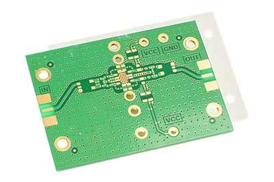
What is ENIPIG?
ENIPIG stands for Electroless Nickel Immersion Palladium Immersion Gold. It is a type of surface finish used in printed circuit board (PCB) manufacturing that provides excellent solderability, wear resistance, and reliability. ENIPIG has become increasingly popular in recent years as a high-performance alternative to other surface finishes like ENIG (Electroless Nickel Immersion Gold) and HASL (Hot Air Solder Leveling).
The ENIPIG process involves depositing multiple layers of metal onto the copper pads of a PCB:
-
Electroless Nickel (Ni): A thin layer of nickel is deposited onto the copper using an auto-catalytic chemical process. This layer provides a diffusion barrier and enhances the adhesion of subsequent layers.
-
Immersion Palladium (Pd): A thin layer of palladium is deposited onto the nickel layer through an immersion process. Palladium serves as a barrier to prevent the diffusion of copper into the gold layer and enhances the reliability of the solder joint.
-
Immersion Gold (Au): A final thin layer of gold is deposited onto the palladium layer through an immersion process. The gold layer provides excellent solderability and protects the underlying layers from oxidation.
The typical thickness of each layer in the ENIPIG stack-up is:
| Layer | Thickness (μin) |
|---|---|
| Gold (Au) | 1-5 |
| Palladium (Pd) | 4-12 |
| Nickel (Ni) | 118-236 |
Advantages of ENIPIG
Superior Solderability
ENIPIG provides exceptional solderability compared to other surface finishes. The thin gold layer on the surface ensures excellent wettability and spreadability of solder, resulting in reliable and consistent solder joints. The gold layer also prevents oxidation of the underlying palladium and nickel layers, maintaining solderability even after prolonged storage.
Enhanced Wear Resistance
The hardness and wear resistance of ENIPIG are superior to those of ENIG and HASL. The palladium layer in ENIPIG provides additional hardness and durability, making it suitable for applications that require frequent insertions or exposure to harsh environments. The enhanced wear resistance of ENIPIG extends the life of the PCB and reduces the risk of contact failures.
Improved Reliability
ENIPIG offers improved reliability compared to other surface finishes, particularly in terms of solder joint integrity and resistance to black pad syndrome. The palladium layer in ENIPIG acts as a barrier to prevent the diffusion of copper into the gold layer, which can cause intermetallic compound (IMC) formation and weaken the solder joint. Additionally, the nickel layer in ENIPIG provides a stable base for the palladium and gold layers, minimizing the risk of black pad syndrome, which is a common issue with ENIG.
Compatibility with Lead-Free Soldering
ENIPIG is fully compatible with lead-free soldering processes, which have become increasingly common due to environmental regulations such as the Restriction of Hazardous Substances (RoHS) directive. The gold layer in ENIPIG ensures excellent solderability with lead-free solders, such as SAC305 (Sn-3.0Ag-0.5Cu), without the need for additional surface preparation or activation.
Coplanarity and Flatness
ENIPIG provides excellent coplanarity and flatness of the PCB surface, which is crucial for achieving reliable solder joints, particularly with fine-pitch components and high-density interconnects (HDI). The thin and uniform layers of nickel, palladium, and gold in ENIPIG result in a smooth and even surface that facilitates accurate component placement and reduces the risk of soldering defects.

Applications of ENIPIG
ENIPIG is suitable for a wide range of PCB applications, particularly those that require high reliability, durability, and solderability. Some common applications of ENIPIG include:
Automotive Electronics
ENIPIG is widely used in automotive electronics due to its excellent reliability and resistance to harsh environmental conditions. Automotive PCBs often experience extreme temperatures, vibrations, and exposure to chemicals, making ENIPIG an ideal choice for ensuring the long-term performance of electronic systems in vehicles.
Aerospace and Defense
PCBs used in aerospace and defense applications must meet stringent reliability and durability requirements. ENIPIG provides the necessary wear resistance and solder joint integrity to withstand the demanding conditions encountered in these applications, such as high altitudes, extreme temperatures, and exposure to radiation.
Medical Devices
Medical devices require high reliability and long-term stability to ensure patient safety and effective operation. ENIPIG is suitable for Medical PCBs due to its excellent solderability, resistance to corrosion, and compatibility with lead-free soldering processes. ENIPIG-finished PCBs are commonly used in medical devices such as pacemakers, imaging equipment, and monitoring systems.
Industrial Controls
Industrial control systems often operate in harsh environments and require reliable and durable PCBs. ENIPIG provides the necessary wear resistance and solder joint integrity to ensure the long-term performance of industrial control PCBs, such as those used in automation systems, power plants, and manufacturing equipment.
Consumer Electronics
ENIPIG is also used in consumer electronics, particularly in high-end devices that require excellent solderability and reliability. Examples include smartphones, tablets, laptops, and gaming consoles. ENIPIG’s compatibility with lead-free soldering processes and its ability to provide a smooth and even surface finish make it an attractive choice for consumer electronics PCBs.

ENIPIG Process Flow
The ENIPIG process involves several steps to deposit the nickel, palladium, and gold layers onto the copper pads of a PCB. A typical ENIPIG process flow includes the following steps:
-
Cleaning: The PCB is cleaned to remove any contaminants or oxides from the copper surface. This step is critical to ensure good adhesion of the subsequent layers.
-
Microetching: The copper surface is microetched to roughen it slightly, which enhances the adhesion of the electroless nickel layer.
-
Electroless Nickel Plating: The PCB is immersed in an electroless nickel plating bath, where a thin layer of nickel is deposited onto the copper surface through an auto-catalytic chemical process. The nickel layer provides a diffusion barrier and enhances the adhesion of the subsequent layers.
-
Immersion Palladium Plating: The PCB is immersed in an immersion palladium plating bath, where a thin layer of palladium is deposited onto the nickel layer. The palladium layer acts as a barrier to prevent the diffusion of copper into the gold layer and enhances the reliability of the solder joint.
-
Immersion Gold Plating: The PCB is immersed in an immersion gold plating bath, where a thin layer of gold is deposited onto the palladium layer. The gold layer provides excellent solderability and protects the underlying layers from oxidation.
-
Rinsing and Drying: The PCB is rinsed with deionized water to remove any residual plating chemicals and then dried using hot air or a drying oven.
-
Inspection: The PCB is inspected to ensure that the ENIPIG surface finish meets the required specifications, such as thickness, uniformity, and solderability.

Quality Control and Testing
To ensure the quality and reliability of ENIPIG-finished PCBs, several quality control and testing methods are employed:
Thickness Measurement
The thickness of each layer in the ENIPIG stack-up is critical to its performance. X-ray fluorescence (XRF) spectroscopy is commonly used to measure the thickness of the nickel, palladium, and gold layers. XRF is a non-destructive technique that provides accurate and precise thickness measurements, ensuring that the ENIPIG finish meets the specified requirements.
Solderability Testing
Solderability testing is performed to assess the wettability and spreadability of solder on the ENIPIG surface. The most common solderability test methods include:
- Wetting Balance Test: This test measures the wetting force and time of a solder ball or wire on the ENIPIG surface. The results provide an indication of the solderability and wetting behavior of the surface finish.
- Dip and Look Test: In this test, the PCB is dipped into a solder bath and then visually inspected for the formation of a uniform and continuous solder coating on the ENIPIG surface.
- Solder Spread Test: This test involves applying a controlled amount of solder paste onto the ENIPIG surface and then measuring the spread area of the solder after reflow. The results provide an indication of the solderability and wetting behavior of the surface finish.
Adhesion Testing
Adhesion testing is performed to evaluate the bond strength between the ENIPIG layers and the copper substrate. The most common adhesion test methods include:
- Peel Test: In this test, a strip of the ENIPIG surface is peeled off the PCB using a controlled force. The peel strength is measured and compared to the specified requirements to ensure adequate adhesion.
- Tape Test: A piece of adhesive tape is applied to the ENIPIG surface and then peeled off. The amount of ENIPIG material removed by the tape provides an indication of the adhesion strength.
Porosity Testing
Porosity testing is performed to detect any pinholes or voids in the ENIPIG layers that could compromise the reliability of the surface finish. The most common porosity test methods include:
- Salt Spray Test: The PCB is exposed to a salt spray environment for a specified duration, and then inspected for any signs of corrosion or degradation of the ENIPIG surface.
- Electrographic Test: An electrically conductive solution is applied to the ENIPIG surface, and an electrical current is passed through the solution. Any pinholes or voids in the ENIPIG layers will allow the current to pass through, indicating the presence of porosity.
By employing these quality control and testing methods, PCB manufacturers can ensure that ENIPIG-finished PCBs meet the required specifications and provide reliable performance in the intended applications.
Comparison with Other Surface Finishes
ENIPIG is one of several surface finish options available for PCBs. It is essential to understand how ENIPIG compares to other common surface finishes to make an informed decision when selecting the most suitable finish for a given application.
ENIPIG vs. ENIG
ENIG (Electroless Nickel Immersion Gold) is another popular surface finish that involves depositing a layer of nickel followed by a layer of gold onto the copper pads. The main differences between ENIPIG and ENIG are:
- ENIPIG has an additional palladium layer between the nickel and gold layers, which provides improved reliability and resistance to black pad syndrome.
- ENIPIG offers better wear resistance and durability compared to ENIG due to the presence of the palladium layer.
- ENIPIG provides superior solderability and wetting behavior compared to ENIG, particularly with lead-free solders.
However, ENIG has some advantages over ENIPIG, such as lower cost and simpler processing, making it suitable for less demanding applications.
ENIPIG vs. HASL
HASL (Hot Air Solder Leveling) is a traditional surface finish that involves dipping the PCB into a molten solder bath and then blowing off the excess solder using hot air. The main differences between ENIPIG and HASL are:
- ENIPIG provides a flatter and more uniform surface finish compared to HASL, which is essential for fine-pitch components and high-density interconnects.
- ENIPIG offers better solderability and wetting behavior compared to HASL, particularly with lead-free solders.
- ENIPIG has a longer shelf life and better resistance to oxidation compared to HASL.
However, HASL is a lower-cost option and is suitable for less demanding applications or those that require a thicker solder coating.
ENIPIG vs. OSP
OSP (Organic Solderability Preservative) is a surface finish that involves applying a thin, organic coating onto the copper pads to prevent oxidation and maintain solderability. The main differences between ENIPIG and OSP are:
- ENIPIG provides a more durable and wear-resistant surface finish compared to OSP, which is essential for applications that require frequent insertions or exposure to harsh environments.
- ENIPIG offers better solderability and wetting behavior compared to OSP, particularly with lead-free solders.
- ENIPIG has a longer shelf life and better resistance to oxidation compared to OSP.
However, OSP is a lower-cost option and is suitable for applications that require a temporary surface finish or those with short storage times before assembly.
FAQ
1. What is the shelf life of ENIPIG-finished PCBs?
The shelf life of ENIPIG-finished PCBs depends on the storage conditions and the thickness of the gold layer. Generally, ENIPIG-finished PCBs can maintain their solderability and performance for up to 12 months when stored in a controlled environment with a temperature of 30°C and a relative humidity of 60%. Thicker gold layers (3-5 μin) can extend the shelf life up to 18 months.
2. Can ENIPIG be used for wire bonding applications?
Yes, ENIPIG is suitable for wire bonding applications. The gold layer in ENIPIG provides an excellent surface for wire bonding, ensuring reliable and stable connections. However, the thickness of the gold layer may need to be adjusted depending on the specific wire bonding requirements, such as the type of wire, bonding temperature, and bonding force.
3. Is ENIPIG compatible with all types of solder paste?
ENIPIG is compatible with most types of solder paste, including lead-free and tin-lead solder pastes. However, it is essential to select a solder paste that is suitable for the specific application and meets the required specifications, such as melting temperature, particle size, and flux activity. It is also recommended to perform compatibility testing to ensure that the solder paste and ENIPIG surface finish provide the desired solderability and reliability.
4. How does ENIPIG compare to ENEPIG in terms of cost and performance?
ENEPIG (Electroless Nickel Electroless Palladium Immersion Gold) is another surface finish that involves depositing a layer of electroless palladium instead of immersion palladium. The main differences between ENIPIG and ENEPIG are:
- ENEPIG typically has a thicker palladium layer compared to ENIPIG, which provides better wear resistance and durability.
- ENEPIG offers slightly better solderability and wetting behavior compared to ENIPIG due to the thicker palladium layer.
- ENEPIG is generally more expensive than ENIPIG due to the additional processing steps and materials required for the electroless palladium deposition.
In terms of performance, both ENIPIG and ENEPIG provide excellent solderability, reliability, and compatibility with lead-free soldering processes. The choice between the two surface finishes depends on the specific application requirements, such as wear resistance, cost, and processing constraints.
5. Can ENIPIG be used for both leaded and lead-free soldering processes?
Yes, ENIPIG is suitable for both leaded and lead-free soldering processes. The gold layer in ENIPIG provides excellent solderability and wetting behavior with both tin-lead and lead-free solders. However, it is essential to select the appropriate soldering parameters, such as temperature profile, dwell time, and cooling rate, based on the specific solder alloy and component requirements to ensure optimal soldering results and reliability.
In conclusion, ENIPIG is an exceptional surface finish technique that offers superior solderability, enhanced wear resistance, and improved reliability compared to other surface finishes. Its compatibility with lead-free soldering processes and suitability for a wide range of applications make it an attractive choice for PCB manufacturers and designers. By understanding the advantages, applications, and processing considerations of ENIPIG, industry professionals can make informed decisions when selecting the most suitable surface finish for their specific requirements.