3D printing technology has progressed tremendously allowing printing not just plastic parts but also advanced functional devices including printed circuit boards. Combining conductive materials alongside insulating polymers allows embedding electronic traces and components directly inside 3D printed constructs.
Let’s get started understanding this progressive additive manufacturing process for embedding electronics.
Overview of 3D Printed Electronics
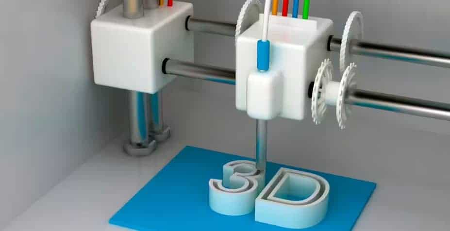
Conventionally, printed circuit boards (PCBs) rely on chemically etching copper foils on flat rigid or flexible insulating substrates. 3D printers open up whole new avenues by extruding conductive material traces encased within insulating thermoplastic builds.
Benefits of such 3D printed electronics include:
Increased Design Freedom – Escape 2D confinement allowing electronics integration onto complex 3D surfaces, flexible substrates and creative form factors.
Rapid Prototyping – Leverage additive manufacturing to quickly iterate over circuit layouts and instantly print next revisions.
Embedded Components – Directly integrate components like sensors, connectors into 3D printed electronics through paused insert molding process.
Less Waste – Additive, precise deposition process unlike traditional PCB fabrication producing large chemical waste streams.
Lower Costs – Eliminate multi-step PCB production, component assembly and lengthy global logistics opening doors for distributed localized production.
As 3D printing technology continues maturing to deliver consistent fine resolution prints alongside new electrically conductive exotic printable formulations, adoption of such direct digital manufacturing techniques for printed electronics will accelerate.
Next let’s look at various materials used.
Conductive Materials for 3D Printing
Conductive interconnections form key building block allowing transmission of signals and power among electronic components.
Metal Fill Filaments – Fused deposition modeling (FDM) printers compatible with thermoplastics can print conductive traces using composite filaments loaded with high percentage of microscopic copper, silver, or graphene particles bonded to the base plastic. Graphene infused nylon or PETg prints offer sheet resistance between 30 to 80 ohms/square making it feasible for digital and analog circuits.
Metal Wire Wrapped – Nylon filament wraps thin stainless steel or copper wire strands around itself during printing creatingraised traces following extruded toolpath. Wired print resolution around 200 microns achieves around 0.01 ohm/sq resistivity adequate for power distribution.
Conductive Ink – Aerosol jetting printers precisely spray specialty silver, carbon or nanoparticle inks through fine deposition nozzles building conductive traces with resistivity as low as 9-10 mohms/square at 10 um print resolution rivaling PCBs.
Liquid Metal Inks – Direct writing tools extrude Gallium Indium based room temperature liquid metal alloy inks hardened through applied voltage building traces with 0.34 mohms/square resistivity retaining flexibility after curing.
So researchers keep widening choices of printable electrically conductive media with competitive resistive performance capable of handling anything from signal transmissions to high power loads.
3D Printing Process for Circuit Boards
Printed circuit boards contain alternating layers of conductive copper traces separated by insulating dielectric substrates. Similarly, 3d printing can build layered electronic packages with embedded conduction paths by precisely dispensing conductive pastes and inks alongside structural thermoplastics layer by layer.
Now let’s explore popular 3D printing processes suitable for embedding electronics – fused deposition modeling (FDM) and stereolithography (SLA).
FDM Process
It’s the most ubiquitous 3D printing technology using spools of thermoplastic filaments like PLA, ABS, nylon as printing media. An extruder heats and precisely deposits them layer by layer based on computer aided design (CAD) toolpaths building up 3D shapes.
Modifications for printed electronics – The extruder swap out between regular insulating filaments and special composite electrically conductive loaded filaments when shuttling between insulating build layers and conductive trace layers per design geometry.
Or coextrusion print heads simultaneously extrude both insulating substrates and conductive traces side by side minimizing inserting to achieve finer resolution and registration accuracy between them.
SLA Printing Process
It relies on photosensitive thermoset resin contained in a vat getting selectively cured and solidified layer by layer using an ultraviolet laser beam tracing slices of the part.
Modifications for printed electronics – Shuttle between regular resin and specialty resin loaded with conductive fillers to build insulating dielectric build material alongside conductive traces. Requires careful calibration and leveling between sequential solidification layers to position traces on substrates.
Finer trace resolution achieved through SLA by using Galvo controlled laser spot versus resolution limited thicker extruded filament traces from nozzle based material extrusion.
Now let’s look at printing builds embedding live electronics.
Creating 3D Prints Embedding Live Electronics
Merely printing conductive traces makes up only half the story for functional printed circuit boards. Embedding electronic components requires additional steps:
Print Base Structure – First print insulating structural body containing cavities matching component shapes using regular thermoplastic materials via FDM or resin if using SLA process.
Insert Components – Next manually populate components like integrated circuits (ICs), resistors, capacitors and connectors into designated holders. Can utilize picked and placed robots for rapid mass assembly.
Pause Print – The print is then paused after automatically detecting insertion of parts.
Print Encasement – Printing resumes by depositing additional filament layers completely embedding the components into the structuring while exposing only their electrical contacts.
Post Processing – For SLA printed boards, further UV oven curing may be needed before washing. They undergo polishing to expose contacts through the resin before adding conductive paint or paste to electrically bridge embedded component pins.
Wiring – Finally wire bonding connects exposed contacts together completing functioning embedded electronic build encompassing both conductive traces and components encased within insulating substrate.
This disruptive insert molding style fabrication process unlocks potential for integrating sensors, circuits, actuators opening up smart product applications.
Applications of 3D Printed Circuit Boards
The intrinsic versatility and customizability of additive manufacturing offer unique opportunities across domains leveraging 3D printed electronics:
Aerospace – Lightweighting complex shaped electronics like antennas while retaining performance. Also repairs and upgrades onboard circuits during extended missions.
Automotive – Custom shaped dashboard electronics matching contours. Also tail light circuits, seat sensors.
Wearables –Embedding electronics by printing directly on textiles or plastics worn close to body. ECG health monitors, sports performance bracelets.
Robotics – Printing stretchable bendable circuits over moving joints of robotic limbs imbuing sensitivity and feedback.
Medical – Custom biosensors for diagnostic Labs-on-a-chip. Also prosthetic limb circuits.
Industrial – Short run IoT sensors, control modules and interconnects replacing PCBs.
Academic Research – Design experiments and frequent layout iterations using in-house printers unlike outsourced PCBs with long lead times.
Rapid Prototyping – Fail fast validation built right on adjusting form factors tailored to user groups before finalization.
As material choices widen alongside printers getting smarter with multi-tool heads and in-process inspection, 3D printing technology will assimilate more steps of electronics manufacturing under one roof.
Pros and Cons of 3D Printed Circuit Boards
Benefits
- Design freedom for organic shapes attaching electronics seamlessly onto 3D contours and enclosures.
- Much faster turn-around with in-house printing versus multi-week PCB fabrication cycles
- Simplified supply chain without dependence on offshore electronics manufacturing hubs.
- Embed components directly inside prints rather than relying on external circuits and wiring harnesses.
- Reconfigure or upgrade circuits by simply printing them afresh with modular designs.
- Build electronic items customized tailored to individuals like prosthetics and wearables.
- Significantly limit material waste generation associated with PCB chemical processing and etching.
- Leverage same CAD models for both electronics and structural mechanical elements reducing integration headaches.
Limitations
- Conductivity and thermal performance of traces lag traditional copper PCBs pending material science advancements.
- Fine pitch precision and reliability still inferior to mature PCB fabrication processes.
- Currently restricted mainly towards low frequency analog sensor circuits given constraints around printing small high density surface mount components needed for digital microelectronics applications.
- Vertical interconnections between layers remain challenging.
- Defect occurrence rates and minimum feature size variabilities still above commercial fab reliability thresholds.
- Requires extensive process refinement and calibrations to achieve repeatable prints.
As technology matures to overcome current shortcomings, 3D printing promises to transform electronics design practices – migrating from designing circuits pegged to rigid two dimensional printed circuit boards towards true three dimensional integrated electrical-mechanical constructs matching exact form, fit and functional requirements.
Challenges Around Adoption of 3D Printed Electronics
While additive manufacturing promises several revolutionary benefits in electronics realms, it also poses unique obstacles needing resolution at both technology and ecosystem level:
Process Factors
Printing resolution – Delivering reliable finer prints nearing trace sizes below 100 microns and matching registration accuracies a must for competitive high density boards.
Fab scalability – Transitioning printers and processes optimized for small batch printing towards high volume production runs mandatory for commercial adoption.
Postprocessing labor – While printer automates fabrication, skilled manual labor still required for intermediate steps like inserting components, sanding, polishing and cleaning. Their cost and throughput also needs optimization for production environments.
Performance benchmarking – Lack of consistent testing standards around key electrical parameters makes it harder for customers to validate quality against application needs.
Printer costs – Industrial grade production 3D printers remain costly to procure limiting startup of printed electronics ventures.
Ecosystem Challenges
Design tools – Insufficient integration of 3D printing rule checks and device simulation into electronic CAD environments hampers designs.
Inertia against change – Getting electrical engineers accustomed to familiar PCB design flows to migrate towards reinventing electronics for 3D platform remains challenging.
Lack of talent – Scarcity of inter-disciplinary skill-sets bridging mechanical and electrical engineering domains slows shift towards embedded electronics.
Regulations – Safety and wireless certifications need overhaul to accommodate direct 3D printed electronics instead of conforming with standards established for conventional PCBs based paradigms.
But the explosive rate of innovations fueled both at material science and additive manufacturing equipment level backed by billions in research investments continues tipping the balance towards printed electronics futures.
Future Outlook for 3D Printed PCBs
Ongoing advances promise exciting possibilities as 3D printing steers towards advanced embedded electronics fabrication:
Hybridized Circuits – Blend direct writing of unusual conductive liquids like gallium alloys alongside pick and place assembly of ICs onto flat thermoplastic films ironing out performance limitations associated with solely additive approaches.
Multimaterial Deposition – Heads with toolchanger arms cycle across disparate filament materials from insulating plastics to metals to inks building embedded laminates with both structural and functional electronics.
In-Process Inspection – Closed loop lysaser aided scans will validate builds between layers flagging defects and adaptively controlling deposition quality on the fly.
Continuous Printing – New paradigm shifts away from per layer intermittent curing allowing continuous flows of programmable smart materials realizing vastly bigger build volumes compared to restricted desktop chambers.
AI Assisted Designs – Generative algorithms customize electronic architectures tailoring to application constraints auto-routing wirelessly connected modules keeping engineers in the loop.
Nanoscale Precision – Leverage self-assembly and directed energy deposition to position microscopic electronic components below tens of microns without reliance on brute force 3d printing resolution advances.
5G Communication Devices – Lightweight flex antennas, sensors and signal conditioning overlays co-fabricated matching curvy platforms through fusion of design, simulation and optimized digital manufacturing workflows.
Myriad pioneers keep challenging status quo faster fabrication and economies of scale effects promise 3D printing is poised to march from being niche rapid prototyping tool today towards mainstream digital manufacturing ecosystems under Industry 5 forward.
Frequently Asked Questions
Here are some common queries regarding 3D printing of electronics:
Q. Can hobby 3D printers print functioning circuits?
DIY kits can print using conductive filaments. But higher end industrial printers are recommended for precision registration printing reliable multi-layer circuits.
Q. Does conductive filament allow soldering components?
It’s tricky to directly solder due to lower melting point. But connectors allow integrating off the shelf components with printed electronics.
Q. How to create Gerber files for printing boards?
Gerber files meant for PCB fabrication cannot directly work. Components need positioning in 3D space using CAD tools respecting assembly order with pause inserts.
Q. Can capacitors and ICs be embedded using extrusion printers?
Challenging since high temperature extrusion damages components. Better results embedding using UV curing SLA printing process instead maintaining lower thermal profiles.
Q. How to add vias between layers in 3D printed circuit boards?
First complete interlayer conductive path using wire or conductive ink dispensing before sealing path with insulating polymers on both entry/exit sides.
So the intrinsic flexibility and automation potential of additive manufacturing can transform making of electronics from time consuming sending of designs for offshore fabrication towards press button desktop manufacturing opening doors for designers, inventors and mad scientists!


0 Comments