Printed circuit boards constitute a significant portion of overall hardware costs in an electronic product. Consequently, minimizing PCB expenditures directly improves project budgets.
In this comprehensive guide, we’ll explore pragmatic techniques to reduce PCB fabrication and assembly costs across areas like:
- Design Simplification
- Build of Materials Optimization
- Supply Chain Strategies
- Manufacturing Tradeoffs
- Volume Consolidation
- Test & Inspection Rationalization
Applying these savings methodologies requires understanding interplay between technical and logistical domains. Let’s jump in examining design considerations!
Simplifying PCB Designs
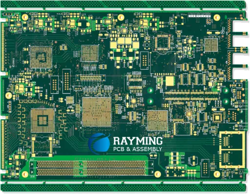
Streamlining board layouts constitutes the most direct path to cost reductions:
Component Reduction – Eliminate non-essential components through design integration. Verify each retained part pulls full weight.
Layer Count Minimization – Utilize least number of conductive layers fulfilling requirements. Additional layers add exponentially more cost.
Dimension Scaling – Shrink boards fitting into retailation panel boundaries to improve panel utilization yields.
Overkill Avoidance – Skip excess specifications that overquality use needs like 6 oz copper weights, immersion gold plating or 1 mil lines.
Standardization – Leverage identical flexible boards across product families when feasible sharing tooling costs through greater volumes.
Design Reuse – Clone common sub-circuits across multiple boards amortizing engineering investments further.
These simplification initiatives streamline production flows allowing scaled savings. Next let’s examine opportunities surrounding components populating boards.
Optimizing Bill of Materials Parts Selection
Which specific components get sourced also provide additional cost control points:
Substitute Alternatives – Swap expensive or scarce parts with cheaper drop-in replacements offering acceptable tradeoffs.
Standardize Families – Consolidate component types, package sizes and pitches when possible across builds.
Eliminate Exotics – Avoid low volume oddball parts challenging procurement. Check market availability before specifying.
Leverage Surplus – Incorporate write-off or excess inventory components accumulation avoiding disposal fees.
Relax Tolerances – Specify wider operating temperature, supply voltage or precision timing windows allowing cheaper material grades.
Review Obsolescence – Gamble with near end-of-life components despite availability risks for huge savings.
Weigh such BOM optimizations against schedule delays if needing full requalification. Now let’s ascend to high level supply chain maneuvers.
Supply Chain Cost Reduction Opportunities
Zooming outwards reveals additional cost-relevant leverage points:
Supplier Diversification – Collect and compare quotes from an expanded range of prospective vendors.
Forward Volume Commitments – Offer defined purchase quantity guarantees with suppliers as negotiation trade items.
Batch Purchases – Consolidate requirements across programs for aggregated orders allowing volume tier discounts.
Consignment Agreements – Secure consignment terms from fabricators and distributors storing your paid inventory until drawn down.
Payment Schedule Stretching – Extend accounts payable cycles through vendor agreements to preserve capital longer.
Low Cost Regions – Shift sourcing to suppliers operating in tax advantaged countries with cheaper labor, facilities or shipping expenses.
While balancing against quality risks, restructuring contractual logistics amplifies cost controls even further. Next let’s dive deeper into manufacturing processes.
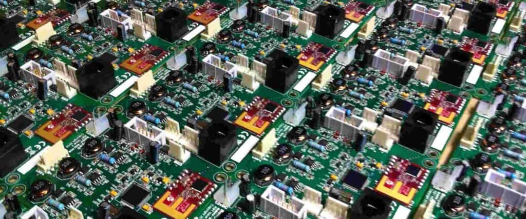
PCB Design Manufacturing Tradeoffs
Deeper manufacturing relationships reveal additional cost-relevant technical considerations:
Layer Thickness – Thinner copper layers save bulk material albeit at higher resistances per unit area.
Soldermask Cuts – Eliminate solder masking beneath large components saving processing steps without compromising insulation.
Finished Copper Edge – Forgo expensive immersion gold plating accepting cheaper organic solderability preservative if testing allows.
Via Styles – Compare blind, buried and through-hole via fabrication quotes for lowest option still satisfying electrical connectivity needs.
Assembly Optimization – Simplify layouts further to reduce component placement, solder paste volumes and simplify vision recognition.
Test Point Population – Reduce excess probing contacts only needed for initial bring-up debugging rather than end-use.
By tailoring designs closer to finalized manufacturing requirements, additional cost fat gets trimmed through tuned fabrication and assembly flows. Now let’s explore consolidating output across programs.
Leveraging Economies of Scale
Amortizing fixed manufacturing investments across larger volumes unlocks substantial cost benefits through:
Panel Loading – Populate actual square area ratio used per panel focusing on common board sizes when applicable.
Batch Standardization – Agree to bulk order using regular monthly or quarterly factory scheduling to synchronize builds across programs leveraging collective volumes securing lower pricing tiers.
Dedicated Tooling – Providing partnership commitments for defined term programs justifies fabricators investing in customized tooling, masking and routing to speed your production.
Extended Life Cycles – Minimize engineering change churn allowing mature designs to yield savings over longer stable manufacturing stretches.
Zero Surplus Agreements – Guarantee purchasing 100% of finished panel inventory within agreed upon terms avoiding write downs.
Panel packing density factors hugely when amortizing production costs. Finally let’s examine quality control reductions possible as confidence increases.
Streamlining Testing and Inspections
As defects drop exponentially through manufacturing maturity, eventually marginal costs outweighing meager quality improvements. Here are areas to trim judiciously:
Reduced Sampling Rates – Slash percentages of tested units as overall batch yield rates consistently exceed targets.
Consolidated Testing – Combine similar verification routines into single comprehensive checkpoint saving duplicate steps.
Relaxed Tolerances – Widen timing, voltage, precision or leakage thresholds as evidence supports without compromising end device functionality given real world operating conditions.
Focused Metrology – Eliminate measurement steps only relevant to initial process capability commissioning but no longer informative long term.
Superior Bin Blending – Relax aesthetic quality bars allowing superior finished goods salvaging by tolerating minor blemishes not affecting functionality.
Skip Final Inspections – Trust proven process integrity enough to ship units immediately without costly final audits and potential rework loops.
Detailed data-driven analysis balancing risks frequently reveal lucrative testing and inspection simplifications possible over time as fundamental manufacturing processes season.
In closing, thoughtfully navigating tradeoffs spanning electrical, mechanical and logistical domains opens multiple avenues for subtracting unnecessary costs from PCB production. What savings strategies have you uncovered? Please share your insights with fellow designers! Now let’s recap some key questions surrounding additional techniques.
PCB Cost Savings FAQs
How much pricing difference splits domestic versus offshore regions?
Historically offshore manufacturers quote approximately 60% less than American fabricators given lower Chinese labor, facilities and regulatory costs but gaps continue narrowing as geopolitical priorities balance reshoring momentum against maintaining strategic domestic competencies.
What are typical panel utilization rates?
PCBA assembly shops expect designers filling 60-75% of panel areas for board sizes under 100 square inches, and 85-90% density for larger boards to maximize capital equipment investments by keeping placement machines continuously populated.
What metrics best forecast cost reduction expectations over time?
Monitor defect parts per million (DPPM) dark hole trends observed across thousands of unique PCBA builds annually. Six sigma practitioners target achieving 100-500 DPPM representing less than 5 defects per every 10 boards allowing intense final inspection reductions.
Which emerging innovations show promise?
Additive multi-beam maskless lithography promises simplifying fabrication initially for advanced HDI flex boards, while thermocompression bonding bypassing solder should bolster reliability and throughput during component attach for mission critical assemblies. Both innovations aim enhancing quality while subtracting costs longer term across entire electronics supply chains touching consumers and infrastructure providers alike ultimately.
With budgets tightening amid volatile materials and transportation costs, scrutinizing every facet of printed circuit technology flows promises eking out additional savings passed onto customers. Please share below any other creative ideas toward optimizing PCB and assembly economics for mutual benefit!


0 Comments