In the ever-evolving world of electronics, the ability to design and fabricate custom printed circuit boards (PCBs) has become increasingly accessible to hobbyists, makers, and enthusiasts. While professional PCB manufacturing services are widely available, etching your own PCBs can be an enjoyable and rewarding process, allowing you to bring your electronic projects to life with a unique personal touch.
Etching PCBs at home not only fosters creativity and hands-on learning but also provides a cost-effective solution for prototyping and small-scale production. In this comprehensive guide, we will explore the step-by-step process of etching your own PCBs, covering materials, techniques, safety considerations, and best practices.
Materials and Tools Required
Before diving into the etching process, it’s essential to gather the necessary materials and tools. Here’s a list of the commonly required items:
- PCB Blanks: These are copper-clad fiberglass boards that serve as the base for your PCB design. They are available in various sizes and copper thicknesses.
- Etchant Solution: The etchant solution is a chemical compound that removes the unwanted copper from the PCB blank, leaving behind the desired circuit pattern. Common etchants include ferric chloride, ammonium persulfate, and sodium persulfate.
- Resist Material: The resist material protects the areas of the copper foil that are intended to remain on the PCB. It can be in the form of a dry film photoresist, a UV-sensitive resist, or a toner transfer method.
- UV Exposure Unit (for Photoresist): If using a photoresist, a UV exposure unit is required to transfer the circuit pattern onto the resist material.
- Etchant Tank or Tray: A suitable container or tray is needed to hold the etchant solution and the PCB during the etching process.
- Agitation Tools: These tools, such as plastic or wooden sticks, are used to gently agitate the etchant solution during the etching process, ensuring even etching.
- Personal Protective Equipment (PPE): Safety gear, including gloves, goggles, and an apron, is essential when handling chemicals and etchants.
- Drill and Drill Bits: After etching, a drill is used to create holes for component leads and vias on the PCB.
- Deburring Tools: These tools, such as files or deburring tools, are used to remove any burrs or rough edges from the drilled holes.
- Cleaning Supplies: Isopropyl alcohol, acetone, or other cleaning agents may be required to remove any residues or contaminants from the PCB after etching.
Step-by-Step Etching Process
Now that you have gathered all the necessary materials and tools, let’s dive into the step-by-step process of etching your own PCB:
1. Design and Prepare the Circuit Pattern
The first step is to design your circuit pattern using PCB design software or create a physical mask using a transparent film or a toner transfer method. Ensure that your design is compatible with the PCB blank size and copper thickness you plan to use.
2. Apply the Resist Material
Depending on the resist method you choose, follow the appropriate steps to apply the resist material to the PCB blank:
- Dry Film Photoresist: Apply the dry film photoresist to the copper-clad side of the PCB blank, ensuring proper adhesion and removing any air bubbles.
- UV-Sensitive Resist: Coat the copper-clad side of the PCB blank with the UV-sensitive resist using a brush or a spin-coating technique.
- Toner Transfer Method: Print your circuit pattern onto a transfer material (e.g., glossy paper) using a laser printer, then transfer the toner pattern onto the copper-clad side of the PCB blank using heat and pressure.
3. Expose the Resist Material
If using a photoresist or UV-sensitive resist, expose the resist material to UV light through your circuit pattern mask or transparency film. This step polymerizes the exposed areas of the resist, making them resistant to the etchant solution.
4. Develop the Resist
After exposure, develop the resist by removing the unexposed areas using the appropriate developer solution or water (depending on the resist type). This step reveals the areas of the copper foil that will be etched away.
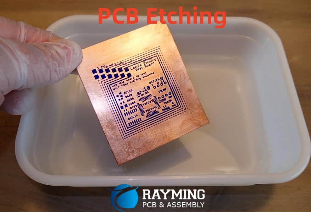
5. Etch the PCB
Prepare the etchant solution according to the manufacturer’s instructions and pour it into the etchant tank or tray. Gently place the PCB into the etchant solution and use agitation tools to ensure even etching. Monitor the etching process closely, as the time required may vary depending on the etchant type and temperature.
6. Rinse and Remove the Resist
Once the etching process is complete, remove the PCB from the etchant solution and rinse it thoroughly with water to stop the etching process and remove any remaining etchant. If using a photoresist or toner transfer method, remove the resist material using appropriate solvents or strippers.
7. Drill Holes
After etching, use a drill press or a handheld drill to create holes for component leads, vias, and other necessary openings in the PCB. Ensure that you use the correct drill bit sizes and follow proper safety precautions.
8. Deburr and Clean
Once the holes are drilled, use deburring tools to remove any burrs or rough edges around the holes. Clean the PCB thoroughly using isopropyl alcohol, acetone, or other cleaning agents to remove any residues or contaminants.
9. (Optional) Surface Finishing
Depending on your requirements, you may choose to apply a surface finish to the PCB, such as solder mask or plating. These processes can enhance the PCB’s appearance, protect the copper traces, and improve solderability.
Safety Considerations
Etching PCBs at home involves handling chemicals and etchants, which can pose potential health and safety risks. It is crucial to follow proper safety precautions and take necessary measures to protect yourself and your surroundings:
- Personal Protective Equipment (PPE): Always wear appropriate PPE, including chemical-resistant gloves, goggles or safety glasses, and an apron or lab coat, when handling etchants and chemicals.
- Ventilation: Ensure proper ventilation in your work area to avoid inhaling fumes or vapors from the etchant solutions and chemicals.
- Chemical Handling and Storage: Follow the manufacturer’s instructions for safe handling, storage, and disposal of etchants and chemicals. Store them in properly labeled containers and keep them away from heat sources, food, and drinks.
- Spill Containment: Have a spill containment kit readily available in case of accidental spills. Follow proper cleanup procedures and dispose of any contaminated materials according to local regulations.
- First Aid Measures: Keep a well-stocked first aid kit nearby and familiarize yourself with the appropriate first aid measures in case of accidental exposure or injury.
- Workspace Setup: Set up your etching workspace in a well-ventilated area, away from potential sources of ignition or heat. Ensure that your work surface is protected and easily cleanable.
- Waste Disposal: Dispose of used etchants, chemicals, and contaminated materials according to local regulations and environmental guidelines. Do not pour etchants or chemicals down drains or dispose of them improperly.
Remember, safety should always be your top priority when etching PCBs at home. If you have any doubts or concerns, consult with professionals or seek guidance from experienced hobbyists or local organizations.
Best Practices and Tips
To ensure a successful and high-quality PCB etching process, consider the following best practices and tips:
- Design Review: Thoroughly review your circuit design before transferring it to the PCB blank. Ensure that all traces, pads, and component footprints are correctly sized and positioned.
- Material Selection: Choose high-quality PCB blanks, etchants, and resist materials to ensure reliable and consistent results. Consider factors such as copper thickness, board material, and chemical compatibility.
- Proper Agitation: Gently agitate the etchant solution during the etching process to ensure even etching and prevent the formation of etchant-resistant films on the copper surface.
- Temperature Control: Maintain the recommended temperature range for the etchant solution, as temperature can affect the etching rate and quality.
- Timing and Monitoring: Closely monitor the etching process and be prepared to remove the PCB from the etchant solution as soon as the desired etching is achieved. Over-etching can lead to excessive copper removal and potential damage to the circuit pattern.
- Thorough Cleaning: After etching, ensure that the PCB is thoroughly cleaned and free of any residual etchant, resist, or contaminants. This step is crucial for ensuring proper component soldering and long-term reliability.
- Practice and Experimentation: Etching PCBs at home is a skill that requires practice and experimentation. Start with simple designs and gradually increase complexity as you gain experience.
- Documentation and Labeling: Maintain accurate documentation of your etching processes, including materials used, etchant concentrations, and exposure times. Label your PCBs with relevant information, such as project names and revision numbers.
- Seek Support and Collaboration: Join online communities, forums, or local maker groups to connect with fellow enthusiasts, share knowledge, and seek advice or troubleshooting assistance.
- Continuous Learning: Embrace a mindset of continuous learning and stay updated with the latest techniques, materials, and best practices in the field of PCB etching and electronics.
Frequently Asked Questions (FAQs)
- Can I etch double-sided PCBs at home? Yes, it is possible to etch double-sided PCBs at home, but the process requires additional steps and techniques, such as properly aligning the circuit patterns on both sides and ensuring even etching across both layers.
- How long does the etching process typically take? The etching time can vary depending on factors such as the etchant solution concentration, temperature, and copper thickness. It can range from a few minutes to several hours. Monitoring the etching process closely is crucial to avoid over-etching or under-etching.
- Can I reuse the etchant solution? Some etchant solutions, such as ferric chloride, can be reused for a limited number of etching cycles. However, it is essential to follow the manufacturer’s recommendations and ensure that the etchant solution remains effective and free of contaminants.
- What is the difference between a resist and a solder mask? A resist is a temporary protective coating used during the etching process to define the circuit pattern on the PCB. A solder mask, on the other hand, is a permanent protective coating applied after etching to insulate the copper traces and define the exposed areas for component soldering.
- Can I etch PCBs with complex designs or high-density components at home? While it is possible to etch complex or high-density PCBs at home, the process becomes more challenging and may require specialized equipment, such as higher-resolution exposure units or tighter design tolerances. For advanced or professional-grade PCB designs, it may be more practical to outsource the manufacturing to a professional PCB fabrication service.
Conclusion
Etching your own PCBs at home is a rewarding and empowering experience that allows you to bring your electronic projects to life with a personal touch. By following the step-by-step process outlined in this guide, gathering the necessary materials and tools, and adhering to safety considerations and best practices, you can successfully etch high-quality PCBs tailored to your specific needs.
While the etching process may seem daunting at first, with practice and experimentation, you will gain valuable skills and knowledge in PCB design, fabrication, and electronics. Embrace the challenges and celebrate the successes, as each etched PCB represents a tangible achievement and a stepping stone towards mastering this fascinating craft.
Remember, etching PCBs at home is not just about creating functional circuits but also about fostering creativity, problem-solving skills, and a deeper understanding of the underlying principles of electronics. So, roll up your sleeves, gather your materials, and embark on this exciting journey of etching your own PCBs!


0 Comments