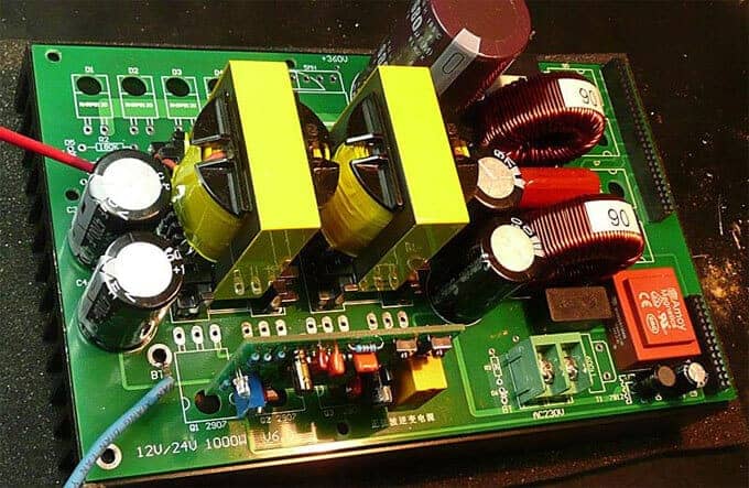
Printed circuit board (PCB) assembly drawings are technical illustrations that provide detailed instructions on how to assemble electronic components onto a PCB. These drawings are a critical part of the PCB design and manufacturing process, ensuring that circuit boards are assembled correctly. This guide will provide an overview of PCB assembly drawings, their key elements, how to read them, and best practices for creating clear, accurate drawings.
What is a PCB Assembly Drawing?
A PCB assembly drawing visually depicts how electronic components like resistors, capacitors, integrated circuits (ICs), connectors etc. are to be placed and soldered onto a PCB. It shows the location, orientation and interconnections for each component. Assembly drawings are created by PCB designers based on the schematics and PCB layout.
These drawings serve as instructions for PCB assemblers, who populate the components onto bare PCBs by hand or using automated assembly machines. They need to precisely understand where and how each component must be mounted. Even small errors in placement or connections can affect functionality.
Clear, accurate assembly drawings are thus essential for assembling functional, high-quality PCBs. They reduce assembly errors and the need for rework. For complex PCBs with hundreds or thousands of parts, assembly drawings are indispensable.
Key Elements of a PCB Assembly Drawing

A good PCB assembly drawing conveys all necessary assembly details in a clear, unambiguous manner. Here are some of the key elements:
1. Reference Designators
Each component on the PCB layout is assigned a unique reference designator like R1, C5, U3, J2 etc. The assembly drawing uses the same designators to identify placement locations for corresponding components. Designators are marked adjacent to component outlines.
2. Component Outlines
Component body outlines visually define the exact placement area for each part on the PCB. Different outline styles indicate component types – rectangular for resistors, circular/oval for capacitors etc. Outlines are drawn to scale.
3. Polarization Markings
Components like electrolytic capacitors, diodes and ICs need to be oriented correctly. Polarization markings (+) show their required orientation. Any assemblies requiring specific orientation are clearly indicated.
4. Bill of Materials
The bill of materials (BOM) lists all components to be mounted, along with designators, values/ratings, and quantities. It serves as a checklist during assembly.
5. Assembly Notes
Supplementary assembly instructions are included as text notes. These cover things like adhesive application, thermal management, sequence of operations etc. Critical notes are highlighted.
6. Board Outline
The board perimeter outline visually defines the boundaries of the PCB. It provides context and scale for component placement.
7. Pin/Hole Locations
Location markings for pins, holes and other board features ensure proper alignment during assembly. Fiducials aid automated assembly.
8. Silkscreen Outlines
The underlying silkscreen legend from the PCB layout file is included as reference. It shows solder pad locations.
9. Assembly Steps
For complex assemblies, sequential procedures are specified using numbered instructions. Step numbers correlate to BOM line items.
How to Read a PCB Assembly Drawing
Being able to properly interpret PCB assembly drawings is key for assemblers and inspection personnel. Here are some tips:
- Understand the meaning of all lines, symbols and notations used in the drawing. Refer to the drafting legend if provided.
- Thoroughly check the BOM and make sure all parts are available before starting assembly.
- Identify component placement locations using their designators marked on the drawing. Verify each part number/value match the BOM.
- Check component orientations against polarization or stagger markings.
- Note the sequence of assembly steps and follow them in order. Pay attention to highlighted special instructions.
- Use assembly notes, silkscreen and fiducials to align PCBs and apply components accurately.
- Insert and solder components using specifications provided for lead trimming, clinching, staking etc.
- Inspect installed parts against drawing before soldering. Catch any errors early.
- Review every detail on the drawing during final inspection after assembly completion.
Best Practices for PCB Assembly Drawings

Well-drafted assembly drawings are vital for assembling complex PCBs right the first time. Here are some best practices for creating quality drawings:
Make it Clear and Uncluttered
Use minimal but precise markings and text. Put extra details in notes. Avoid clutter than can cause confusion.
Use Standard Symbols and Notations
Follow industry standards like IPC for markings. This aids drawing comprehension.
Show Polarization and Orientation
Indicate component quadrant orientation, pin 1 locations etc. fully and unambiguously.
Maintain Correct Scale
Illustrate components and board in proper 1:1 scale. Don’t distort or compress.
Call Out Critical Details
Highlight assembly precautions through text boxes, arrows, borders etc.
Draft It Yourself
Don’t outsource drafting. Component placement knowledge is vital for clarity.
Proofread Thoroughly
Double check all designators, text, BOM agreement and markings systematically.
Include a Drawing Legend
Provide a drawing symbol and notation key for clarity.
Frequently Asked Questions
1. Are assembly drawings necessary for simple PCBs?
For boards with just a few large components, well-marked silkscreen legends may suffice. But assembly drawings are recommended even for low-complexity PCBs to avoid errors and aid inspection.
2. Can assembly drawings assist troubleshooting?
Yes, comparing an assembled board against its drawing helps identify missing, misaligned or incorrect components that may be causing issues. The drawing provides a blueprint for how the assembled PCB should look.
3. What software is used for making assembly drawings?
While CAD programs like Altium, Eagle, OrCAD etc are most commonly used, drawings can also be created using illustration tools like CorelDraw or Illustrator. The key is proper scaling and clarity.
4. Is it advisable to combine assembly and fabrication drawings?
It’s generally better to have separate drawings for PCB assembly and fabrication. Combining them can clutter component placement illustrations. Keeping them separate improves drawing clarity for the assembler.
5. Can assembly drawings assist design-for-manufacturing?
Yes, having clear assembly documentation helps assess manufacturability during design stages itself. Issues like component spacing, orientation, sequence etc can be improved before PCB layout is finalized.
6. Does IPC standard cover assembly drawing symbols?
Yes, the IPC-2615 standard provides guidelines and recommended symbols for PCB assembly drawings. It aims to standardize drafting and markings for clarity.
Conclusion
Well-crafted PCB assembly drawings are indispensable for assembling today’s complex, dense electronic circuits. They provide clear visual instructions so assemblers know exactly where and how to place each component on a PCB. Investing time upfront to create accurate, easy to follow assembly drawings helps prevent costly errors and rework further down the assembly process. With the aid of assembly drawings, PCB assemblers can work efficiently and deliver high functioning boards that matches the intended design.


0 Comments