Introduction to PCB Assembly and Soldering
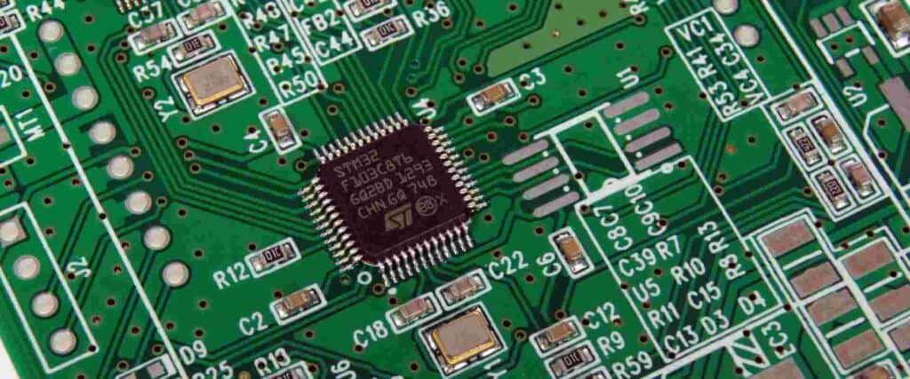
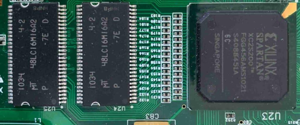
Printed circuit boards (PCBs) are essential components of most modern electronic devices. A PCB mechanically supports and electrically connects electronic components using conductive tracks, pads and other features etched from copper sheets laminated onto a non-conductive substrate. PCB assembly is the process of soldering or assembling the components onto the PCB.
Proper PCB assembly requires high precision soldering and inspection using advanced equipment and skilled technicians. This article provides a comprehensive overview of PCB assembly and soldering services, including the assembly process, soldering techniques, inspection and testing methods. It also covers tips for choosing reliable PCB assembly service providers.
The PCB Assembly Process Step-by-Step
The typical PCB assembly process involves the following key stages:
1. Bill of Materials (BOM) and Assembly Drawing
- The BOM lists all the components required for assembly with reference designators, specifications, quantities and supplier part numbers.
- The assembly drawing or PCBA drawing details the visual placement of the components on the bare PCB.
2. Kitting and Staging Components
- Components are taken from storage, “kitted” based on the BOM and staged for assembly.
- Reels, tubes and trays containing like components are set up at the production line.
3. Solder Paste Stenciling
- A thin layer of solder paste is applied on the bare PCB through a metal stencil using a solder printer.
- The solder paste serves as adhesive to temporarily hold components before soldering.
4. Pick and Place Assembly
- Robotic pick and place machines populate components onto the PCB by “picking” parts from the kits and “placing” them accurately onto the stenciled solder paste.
- Optical alignment and computer vision guide high precision placement.
5. Reflow Soldering
- The populated board goes through a reflow oven to melt the solder paste and form solder joints holding the components.
- The board passes under infrared heaters through preheat, reflow and cooling zones in the conveyorized oven.
6. Inspection and Testing
- Assembled boards are put through optical and x-ray inspection to check for defects. Testing verifies assembly accuracy and functionality.
- Failed boards are reworked or scrapped depending on the defect type and severity.
7. Conformal Coating and Final Finishing
- A protective plastic coating may be applied over the assembled PCB for environmental protection.
- Other finishing steps like trimming, cleaning, labeling and packaging complete the assembly.
Soldering Techniques Used in PCB Assembly
There are several soldering techniques used in assembling PCBs:
- Reflow soldering melts solder paste deposited by stenciling to attach components. It is the most common method.
- Wave soldering flows a wave of molten solder over the bottom side of the board to solder component leads after placement. Used for high volume production.
- Manual soldering using a soldering iron is done for rework, repairs and low volume production.
- Selective soldering focuses heat and solder at the joint area to avoid heating sensitive components. Used for soldering connectors or odd shaped parts.
- Vapor phase soldering condenses hot vapor to uniformly heat the assembly and melt the solder. It provides excellent solder joint quality.
- Laser soldering uses a laser pulse to heat the joint area without contact. Used for small delicate parts and repairs.
The right soldering process depends on factors like volume, component types, quality requirements, capital investment and operating costs.
Inspection and Testing Methods
Thorough inspection and testing ensures quality and reliability of the completed board assembly. This helps catch defects before shipment. Some inspection and testing methods include:
Visual Inspection
- Trained operators visually check the PCB for defects like missing, misaligned or incorrect components, poor solder joints, mars and residue. Aids like magnifying lenses, microscopes and image processing may be used.
X-Ray Inspection
- X-ray imaging reveals hidden defects like shorts, open or insufficient solder joints, voids in solder, bent component leads and so on. Especially useful for inspecting ball grid arrays (BGAs) and other hidden solder joints.
Automatic Optical Inspection (AOI)
- AOI systems take high resolution images that are digitally processed to identify defects based on patterns. AOI finds even tiny defects invisible to the naked eye.
In-Circuit Testing (ICT)
- Probes test electrical nodes, component values and board functionality applying signals and measuring responses. Tests dynamic interactions between components.
Flying Probe Testing
- A “flying probe” makes electrical measurements between test points on moving boards without test fixtures. Checks continuity between nodes rapidly.
Functional Testing
- Running assembled boards under operating conditions verifies that the assembly functions per design. Stressed electrical and environmental testing uncovers latent defects.
Other Tests
- Additional tests like board flexure, shear strength, simulation modeling, thermal analysis and x-ray tomography may be done based on specific quality requirements.
Tips for Choosing a Reliable PCB Assembly Service Provider
Here are some tips for selecting a capable PCB assembly service provider:
- Look for companies with certifications like ISO 9001, IPC membership, ITAR registration etc.
- Evaluate their capabilities – equipment, expertise, technologies, capacity, locations.
- Review quality processes like component sourcing, ESD control, change management.
- Assess design support – DFM recommendations, library support, engineering review.
- Validate capabilities through prototypes before full production.
- Check reference customers, reviews, company financials and track record.
- Compare pricing models like per component, per board or volume discounts.
- Optimize costs through supply chain management and DFM decisions.
- Seek turnkey services encompassing procurement, kitting, assembly, inspection, test and finishing.
- Ensure responsiveness and good project communications.
FQA
What are the benefits of outsourcing PCB assembly rather than in-house assembly?
Outsourcing to an expert PCB assembly service provider offers several benefits compared to in-house assembly:
- Access to the latest equipment, skills and technologies without major capital investment.
- Focus internal resources on core competencies rather than assembly operations.
- Leverage expertise and best practices from experience across projects.
- Scale production up or down flexibly based on demand.
- Reduce costs through collective component procurement.
- Ensure consistent quality with rigorous process controls.
- Get fast turnarounds and rapid prototyping services.
- Shift fixed costs to variable costs based on actual usage.
What documentation is required for outsourced PCB assembly?
The key documentation required includes:
- Bill of Materials listing all components, reference designators, values, specifications, quantities and supplier part numbers
- Assembly drawings showing component placement and orientation on the bare board.
- Component packaging specifications
- Approved Vendor List
- Solder paste stencil or solder mask design files
- Any special assembly notes or instructions
- Test procedures and quality acceptance standards if applicable
How are components procured for PCB assembly?
For full turnkey PCB assembly services, the assembly provider typically procures components required based on the customer’s Bill of Materials. This simplifies the procurement process for the customer.
Components are sourced from the customer’s approved manufacturers list. If alternate sources are needed, the assembler gets approval after validation. Rigorous quality checking of incoming component shipments prevents counterfeit parts entering the production line.
What defects can occur in PCB assemblies?
Some common PCB assembly defects are:
- Missing, wrong or misaligned components
- Wrong component values
- Solder shorts, bridges or insufficient solder
- Solder splatter, webbing or skew
- Damaged PCBs or components
- Cold or cracked solder joints
- Residual flux or foreign object debris
- Board or component warping/bending
- Polarity errors
- Violation of assembly spacing rules
How can defects be minimized in PCB assembly?
Some best practices to minimize defects are:
- Validate and inspect incoming components
- Implement ESD control procedures
- Use no-clean solder paste and eliminate board washing
- Program optimized reflow profiles tailored for the assembly
- Employ precision stencils, accurate pick-and-place machines
- Perform regular maintenance and calibration on assembly equipment
- Implement inspection points after critical steps
- Leverage automated optical, xray and electrical inspection
- Validate processes through upfront prototyping
- Apply corrective actions and continuously improve processes
Conclusion
PCB assembly transforms bare printed circuit boards into fully functioning electronic assemblies using precision component placement, soldering processes, and inspections. Outsourcing to an expert PCB assembly service provider that uses advanced automation, rigorous quality controls and turnkey services enables companies to get high quality assembled boards quickly and cost-effectively. Companies should evaluate the capabilities, expertise, technologies and value provided by potential assembly partners when selecting the right provider for their needs.


0 Comments