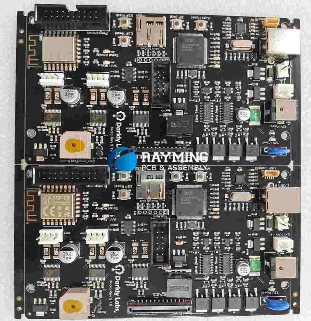
Introduction to PCB Assembly
Printed circuit board (PCB) assembly is the process of soldering electronic components to a PCB. It is an essential step in manufacturing electronic devices. This article will provide a comprehensive overview of PCB assembly, including the key steps, equipment, design considerations, and frequently asked questions.
The PCB Assembly Process
PCB assembly involves several key steps:
1. Solder Paste Printing
Solder paste is applied to the PCB pads where components will be placed. This is usually done using a stencil and solder paste printer. The solder paste creates a temporary bond between the components and PCB.
2. Component Placement

Electronic components are precisely placed on the PCB according to the design schematics. This is automated using pick and place machines for high volume production.
3. Reflow Soldering
The PCB passes through a reflow oven, melting the solder paste and permanently soldering the components in place. Different soldering profiles are used based on the components and PCB design.
4. Inspection and Testing
Once assembled, PCBs undergo electrical testing and visual inspection to verify all connections are properly soldered and there are no defects. Automatic optical inspection (AOI) systems are often used.
5. Conformal Coating
A protective coating is sometimes applied to prevent corrosion and enhance PCB reliability. Conformal coatings are applied by spraying or immersion.
PCB Assembly Equipment
Specialized equipment is used for efficient, high-quality PCB assembly:
- Solder paste printers – Apply solder paste through stencils onto PCBs
- Pick and place machines – Place components rapidly and precisely onto PCBs
- Reflow ovens – Solder components to PCBs by heating solder paste above its melting point
- AOI systems – Inspect PCBs optically for defects
- Functional testers – Verify electrical functionality of assembled PCBs
Key Design Considerations
PCB design significantly impacts the assembly process. Here are some key considerations:
- Component spacing – Adequate spacing between components for pick and place and soldering
- Component orientation – Consistent orientation for easy robot pickup
- Board size – Standard sizes facilitate assembly handling
- Solder mask – Defines soldering areas and component spacing
- Silkscreen – Component designators, polarity markings, etc. for assembly
- Test points – Included for testing assembled boards
Table summarizing key PCB design considerations:
| Consideration | Description |
|---|---|
| Component spacing | Adequate spacing for manufacturing |
| Component orientation | Consistent for easy robot pickup |
| Board size | Standard sizes facilitate handling |
| Solder mask | Defines solder areas and spacing |
| Silkscreen | Assembly markings and labels |
| Test points | For testing assembled boards |
PCB Assembly Process FQA
Here are some frequently asked questions about PCB assembly:
1. What is the typical tolerance for component placement?
The component placement tolerance is generally +/- 0.1 mm or less for surface mount and +/- 0.5 mm for through-hole components. High precision pick and place machines can achieve tolerances down to 50 microns.
2. How are very small components like 0201 chips handled?
Specialized pick and place heads with vacuum nozzles are used to handle tiny 0201 and 01005 components. Camera systems precisely locate the components.
3. How are solder joints inspected?
Automated optical inspection (AOI) is commonly used to check solder joint integrity. X-ray inspection provides detailed views of hidden solder joints.
4. What is head-in-pillow defect?
Head-in-pillow defect occurs when an IC is misaligned inside the solder joint. This can lead to cracked joints and electrical failure.
5. How can PCB assembly quality be improved?
Optimizing solder paste printing, component placement, and reflow profiling improves quality. Temperature profiling, AOI, and regular machine calibration also help significantly.
This covers the key steps, equipment, design factors, and FAQs related to PCB assembly. Proper assembly is vital for creating reliable, high-performing electronic products. With attention to detail in the design and manufacturing process, companies can build leading-edge electronic devices using PCB assembly.


0 Comments