Introduction
Printed circuit boards (PCBs) are essential components in nearly every electronic device. As products become smaller and more complex, engineers are turning to flexible PCBs (flex PCBs) as solutions. Flex PCBs offer a number of advantages over traditional rigid boards including flexibility, space savings, and improved reliability. However, designing and producing flex PCB prototypes presents unique challenges. This guide will provide a comprehensive overview of flex PCB prototyping including design considerations, manufacturing processes, and testing. With the right approach, engineers can utilize flex PCB prototypes to evaluate and refine their designs quickly and cost-effectively.
Design Process and Considerations
The design process for a flex PCB prototype shares similarities with that of a standard PCB, but the flexible nature requires additional considerations:
Substrate Selection
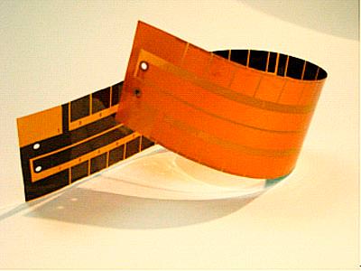
The flexible substrate or base material is a key design choice. Polyimide films such as Kapton or Upilex are commonly used. Thinner materials down to 12.5 microns allow for tight bend radii. In high-frequency or high-speed designs, materials with low dielectric loss are preferred.
Layer Stackup
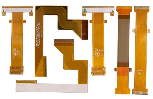
Determining the layer stackup is important for mechanical performance. A common stackup begins with a polyimide base, followed by a thin copper layer, adhesive layer, and another polyimide layer. The number of layers can be increased as needed.
Bend Radius
A primary constraint is the minimum bend radius the flex PCB can tolerate. This is a function of the substrate, copper thickness, and stackup. Tighter bend radii improve flexibility but increase stresses.
Stiffener Integration
Strategically placed stiffeners made from materials like polycarbonate can be added to maintain stability and prevent flexing in certain areas.
Electrical Rules
It’s critical to follow trace width/spacing rules for impedance control and prevent shorts during flexing. Wider traces and spaces may be required.
Connectors and Vias
Special care should be taken with connectors and vias in flexing regions to prevent cracking. Measures like extra padding around vias can help.
3D Modeling
Modeling and simulation with software tools can identify physical stresses and clashes early in the design phase.
Prototype Manufacturing Process
Once the flex PCB design is complete, producing prototypes requires specialized manufacturing techniques:
Imaging
A laser direct imaging (LDI) system exposes a photosensitive layer on the flex substrate material to define traces and features. Phototools are not required.
Etching
Etching removes unwanted copper to leave only the desired traces. Flex PCBs often require stress relief etching to prevent damage.
Coverlay Application
Coverlay, a solder mask-like polymer layer, is applied over the traces for insulation and to prevent copper wicking.
Rigid-Flex Processing
For rigid-flex boards, sections needing stiffness are processed through separate rigid PCB steps.
Assembly
Surface mount and thru-hole components can be assembled similarly to rigid boards. Care is required during soldering to avoid damaging flex areas.
Testing
Inspection tests like automated optical inspection (AOI) combined with electrical testing verifies the prototype’s design and quality.
Cutting
A range of methods from razor blades to precision lasers can separate individual flex PCBs from panels.
Prototype Testing
Thoroughly testing prototypes is key to catching design flaws and confirming flex performance:
Functional Testing
Validate basic functionality by powering on the board and testing operation of components and circuits.
Physical Manipulation
Bend, twist, and manipulate the flex PCB through anticipated motions to check for electrical faults or physical damage.
Environmental Stress
Subject prototypes to expected environmental conditions such as temperature cycling, vibration, and humidity to uncover weaknesses.
Specification Validation
Verify that performance meets requirements for parameters like impedance, transmission speeds, noise, and emissions.
Cycle Testing
Repeatedly flex circuits over an extended period to simulate wear and check for degradation or failure.
3D Scanning
Use scanning to model and digitally inspect PCBs in different flexed states for insights into stresses and failures.
With rigorous testing, flaws in design or manufacturing can be identified in prototypes rather than finished products.
Key Prototyping Considerations
Here are some high-level best practices to consider for flex PCB prototyping:
- Closely involve your flex PCB manufacturer early in the design process. Their expertise in manufacturability and available capabilities is essential.
- Build in adequate time for prototyping iterations to test and refine the design. Be prepared to go through multiple revisions.
- Focus on reliability testing such as HAST, temperature cycling, and vibration early to uncover potential weaknesses.
- Modeling and simulation with FEA tools takes time but pays dividends for anticipating issues before manufacturing.
- Consider using simpler substrates like polyimide for quick early prototyping iterations before moving to more advanced materials.
- Don’t cut corners on QA steps like electrical testing and inspection. This ensures high prototype quality.
Prototyping done right provides the feedback to develop a robust flex PCB design while avoiding costly mistakes.
Flex PCB Prototyping FAQ
Here are some frequently asked questions about flex PCB prototyping:
Q: How long does it typically take to get flex PCB prototypes produced?
A: With an experienced flex PCB manufacturer, functional prototypes can often be delivered in 5-7 days. More complex designs with rigid-flex require 10-15 days.
Q: What are some key benefits of prototyping with flex PCBs versus breadboards or rigid PCBs?
A: Flex PCB prototypes reflect the true design much more accurately in terms of electrical performance and physical characteristics. Flexing can be fully validated.
Q: What design tools are most important for flex PCB prototyping?
A: 3D CAD modeling and FEA tools are critical for simulating physical stresses. For electrical design, constraints driven layout and impedance tuning help match models.
Q: What are some important guidelines for selecting connectors and components?
A: Avoid large connectors. Prioritize compact surface mount parts rated for flex applications. Underfill connectors in flex areas to prevent cracking.
Q: How many prototype iterations should be planned for a complex flex design?
A: Most designs require at least 2-3 iterations to refine the layout, stackup, bending dynamics, and electrical performance. More complex systems may need 5+ iterations.
Conclusion
This guide covers key considerations, processes, and best practices for flex PCB prototyping. With careful planning and execution, flex PCB prototypes enable validation of designs and improvements prior to full production. Prototyping is essential for realizing the benefits of flex PCBs like reliability, small form factors, and dynamic movement in finished products. By partnering with an experienced flex PCB manufacturer and following the steps outlined here, engineers can develop robust and optimized flex PCB designs.


0 Comments