Designing Circuit Card Assemblies for Optimal Performance
Introduction
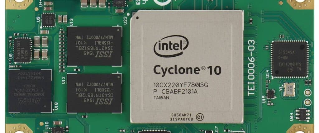
Circuit card assemblies (CCAs), also known as printed circuit boards (PCBs), serve as the foundation for electronic devices and systems. Proper CCA design is critical for ensuring optimal performance, reliability, and manufacturability of the final product. This article provides an overview of key considerations and best practices for designing robust, high-quality CCAs.
Component Placement and Routing
The physical layout of components and routing of traces on a CCA can significantly impact performance and manufacturability. Some key guidelines include:
- Group related components together – Keep associated components like integrated circuits with their support components together instead of spreading them out across the board. This helps minimize trace lengths.
- Prioritize critical traces – Ensure the highest speed or most noise-sensitive traces have priority in routing. These should be kept as short and direct as possible.
- Maintain symmetry – Strive for symmetry in component placement and routing to minimize skew between differential pairs.
- Allow for thermal relief – Leave adequate spacing around high-power components to allow heat dissipation. Avoid placing them in tightly confined spaces.
- Facilitate testability – Leave test points to facilitate testing and debugging. Provide adequate access to programmable components.
- Limit crossing traces – Minimize the number of traces that cross over others. Use vias to transition between layers when necessary.
Layer Stackup
The layer stackup, or sequence of copper and dielectric layers in a multilayer board, must be properly engineered to meet performance and manufacturability objectives:
- Control impedance – Match trace width and spacing to dielectric thickness to achieve target impedance (often 50-ohms for high-speed signals).
- Minimize plane splits – Avoid unnecessary splits in power and ground planes which act as return paths.
- Provide shielding – Incorporate shielding layers adjacent to critical traces to isolate them.
- Balance layer distribution – Strive for equal numbers of signal layers in each half of the stackup to avoid warping.
- Limit layer transitions – Minimize the number of times critical traces transition between layers. Each transition adds impedance discontinuity.
- Allocate layers wisely – Use thicker copper and dielectric layers deeper in the stackup since they are less prone to etching issues during manufacturing.
Example 4-Layer Stackup
| Layer | Function |
|---|---|
| Top | Signal |
| 2 | Ground Plane |
| 3 | Power Plane |
| Bottom | Signal |
Bypassing and Decoupling
Proper power distribution design is crucial for maintaining integrity of power supply voltages in a CCA. Two key techniques are:
- Bypassing – Connecting bypass capacitors directly between the power and ground pins of active devices. This provides localized charge storage.
- Decoupling – Using decoupling capacitors distributed across the board connected to power/ground planes. This dampens power supply noise.
Guidelines for effective bypassing and decoupling:
- Use low ESL/ESR ceramic capacitors designed for high frequency bypassing.
- Place bypass caps as close as possible to IC power pins.
- Use a mix of values (0.1uF, 1uF, 10uF etc) to target a wide frequency range.
- Provide multiple vias to minimize inductance to power and ground planes.
- Include some electrolytic capacitors for bulk decoupling in parallel.
Signal Integrity
Managing signal integrity through controlled impedance routing and termination is key to minimizing signal degradation.
- Matched impedance – Route traces over a continuous ground plane and match trace width to dielectric thickness to control impedance.
- Minimize stubs – Avoid stubs (short branches) on critical traces which cause reflections.
- Proper termination – Use resistor termination matched to trace impedance at signal destinations.
- Careful clock routing – Clock signals should be treated as critical nets with proper impedance control and termination.
Thermal Management
Careful thermal design avoids issues with components overheating:
- Thermal vias – Incorporate thermal vias under hot components to conduct heat away into inner board layers.
- Plane layers – Use continuous copper planes for heat spreading. Inner layers conduct and spread heat more effectively.
- Heatsinks and cooling – For very high power components, use heatsinks, fans or liquid cooling.
- Board thermals – Monitor board temperature during operation and use thermal simulation to identify hotspots.
Material Selection
Proper material selection balances performance, reliability, and cost:
- Dielectrics – FR-4 is suitable for many designs. High frequency boards may require low-loss laminates.
- Copper thickness – 1 oz copper is standard. 2 oz or thicker copper may be needed for high current designs.
- Finishes – Immersion silver, ENIG, and HASL are common surface finishes. Evaluate compatibility with components.
- Solder mask – Use solder mask definable processes for tight tolerance. LPI and laser direct imaging are options.
Design for Manufacturing (DFM)
- Board size – Standard panel sizes are 12 x 18”, 16 x 24”, 18 x 24”. Custom sizes can be more expensive.
- Component sizes – Use standard metric component sizes for easier sourcing. Avoid hard-to-find imperial sized parts.
- Tolerances – Design rules must account for tolerances in fab and assembly processes.
- Test points – Include testpoints for validation and debugging of the assembly.
- Lead-free – Use lead-free components and lead-free soldering processes.
Design for Test (DFT)
- Test points – Provide test points to access key nodes for verification.
- JTAG/Boundary scan – Implement boundary scan chains for simplified board-level testing.
- Built-in diagnostics – Include on-chip diagnostic circuitry to report errors.
- Event logging – Maintain event logs to record anomalies and faults.
- Third-party tools – Utilize tools like LabView, dSPACE or internal scopes for system-level testing.
By following design best practices and guidelines, circuit card assemblies can achieve optimal functionality, performance, reliability, and manufacturability. Paying attention to details like layout, decoupling, layer stackup, signal integrity, thermal design, and design for manufacturing/test ensures a robust end product.
Frequently Asked Questions
What are some key goals in designing circuit card assemblies?
Some of the key design goals include:
- Achieving target functionality and performance specifications
- Optimizing signal integrity by controlling impedance, minimizing reflections etc.
- Allowing for effective heat dissipation through thermal design
- Enabling design for manufacturability by standardizing components, board sizes etc.
- Facilitating design for test via testpoints, boundary scan etc.
- Ensuring reliability under expected operating conditions
- Meeting cost targets by balancing performance and manufacturability
How can Poor CCA design impact performance?
Poor CCA design can negatively impact performance in various ways, including:
- Excessive trace lengths leading to increased parasitic resistance/capacitance
- Asymmetric routing causing signal skew between differential pairs
- Improper layer stackup resulting in impedance mismatches and reflections
- Power supply noise due to inadequate decoupling or bypassing
- Thermal issues from heat buildup and hotspots
- Uncontrolled impedance leading to signal degradation
- Manufacturing defects from lack of design margin and tolerances
What are some key factors in selecting PCB materials?
Some key considerations in selecting PCB materials include:
- Dielectric constant and loss – impacts signal integrity at high frequencies
- Thermal conductivity – ability to conduct heat away from hot components
- CTE coefficient – match CTE to that of components to minimize warping and thermal stress
- Moisture absorption – absorptivity affects dimensional stability and reliability
- Copper thickness – impacts allowable current carrying capacity
- Mechanical characteristics – influences physical robustness and flex tolerance
- Chemical compatibility – resistance to processes like soldering and cleaning
- Cost – striking optimal balance between cost and performance
How can signal integrity be maintained in CCA design?
Some ways to maintain signal integrity in CCA design are:
- Matched impedance routing using controlled trace widths and dielectric materials
- Minimizing stubs through optimal component placement and routing
- Proper termination of transmission lines using resistor matching line impedance
- Careful treatment of clock signals as high-speed critical nets
- Using planes for shielding sensitive traces from noise sources
- Limiting transitions across layers which cause impedance discontinuities
- Providing adequate local charge storage through bypassing techniques
- Simulation of key traces to identify and correct signal degradation
What are some key thermal management strategies for CCAs?
Key CCA thermal management strategies include:
- Incorporating thermal vias under hot components to conduct heat into board
- Using continuous inner layer copper planes to spread heat over area
- Allowing sufficient spacing around high-power components
- Mounting heat sinks or cold plates on top of hot components
- Using fans/blowers focused on hot areas
- Implementing liquid cooling for very high heat densities
- Monitoring board temperature using embedded thermal sensors
- Performing thermal simulation to map expected hot spots


0 Comments