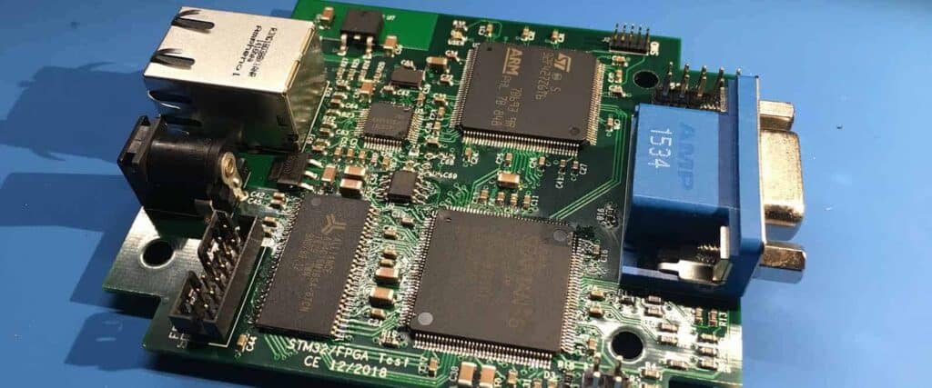
Altium Designer is an electronic design software that allows designers to create complex printed circuit boards (PCBs) and systems from concept through to manufacturing. One of its powerful features is the ability to design and assemble multi-board systems, enabling the integration of multiple interconnected circuit boards. This provides flexibility to divide complex designs across multiple boards while still designing and visualizing the overall system connectivity.
Benefits of Multi Board Design in Altium
Designing multi board systems in Altium provides several advantages:
Simplify Complex Designs
Large, intricate systems can be partitioned across separate PCBs to simplify routing, component placement, and design work. This modular approach divides the design complexity and allows focus on individual board sections.
Facilitate Team Collaboration
Different sections of a multi board system can be assigned to separate designers or teams. This enables concurrent design work and collaboration for faster development.
Improve Manufacturability
Multiple smaller boards can be easier and cheaper to fabricate compared to one large, complex board. Individual boards can use different materials and processes as needed.
Enable Design Reuse
Common sections like power supplies or I/O interfaces can be designed once then reused across boards. This saves design time and ensures consistency.
Support Assembly/Serviceability
System sections on separate boards can be independently assembled, tested, serviced and replaced as needed. This facilitates manufacturing and maintenance.
Optimize Form Factor
Partitioning allows flexibility to optimize board shapes and footprints. This can help create products with compact, space-efficient form factors.
Multi Board Design Process in Altium

Designing a multi board system requires coordination across boards at the component, schematic, and PCB levels. Here is an overview of the multi board design workflow in Altium:
1. Plan System Architecture
First, define the overall system architecture – determine board functions, layout, and partitioning of components/circuits across boards.
2. Create Project and Design Files
Set up an overall project for the multi board system. Create separate schematic and PCB files for each board within the project.
3. Design Individual Boards
For each board, complete the normal electronics design process: create schematics, select components, route PCBs, etc.
4. Define Board-to-Board Interfaces
Determine the signal, power, and mechanical connections between boards. Design matching connectors, cables, and ports.
5. Develop Board Stackup
Coordinate board layer stacks, materials, and geometry between boards that will interface. Account for physical clearance.
6. Combine Boards into System
In the main project, add the separate board files. Review system connectivity via schematic sheets and 3D PCB editor.
7. Generate Manufacturing Outputs
Run design rule checks on individual boards and the overall system. Generate fabrication and assembly files for manufacturing.
Multi Board System Design Features in Altium
Altium provides integrated features and workflows to facilitate the design of complex, interconnected multi board systems:
Schematic Partitioning
Large schematics can be divided into multiple sheets within or across schematic files. Sheets can be linked with off-sheet connectors to visualize system connectivity.
Multi-Channel Design
Functional blocks of a system can be isolated into separate channels to clearly organize and manage multi board architectures.
Cross Probe Navigation
Navigate and cross probe between matching circuits and components across schematic sheets and board designs. Easily explore design connectivity.
Multi-Board CAD Environment
Visualize and arrange multiple boards together in a system assembly in the 3D PCB editor. Define board shapes, spacing, alignments, etc.
Rigid-Flex Support
Model multi-layer rigid and flex sections within a single PCB or across multiple boards using rigid-flex design rules.
Multi-Board BOM Generation
Combine component requirements across all boards in a system into compiled multi-board BOM reports for procurement and assembly.
Multi-Board Manufacturing Outputs
Generate manufacturing and assembly files for the overall system, including netlists, bill of materials, fabrication drawings, and assembly drawings.
Multi Board Assembly Techniques

In addition to design, multi board systems require careful planning for system assembly. Some key assembly techniques used with Altium multi board designs include:
Board Stacking with Standoffs
Boards can be physically stacked and aligned using screw-mounted standoff spacers between boards. Allows compact 3D arrangement.
Inter-Board Connectors
Board-to-board connectors soldered on each PCB provide mechanical and electrical connections. Examples are board-stacking connectors, mezzanine connectors.
Flexible Interconnects
Flex cables can connect PCBs and allow movement/flexing between rigid boards. Useful in applications like laptops.
Board-to-Board Shield Stacks
Some systems are assembled by plugging daughter boards onto motherboards via shield connectors. Example is Arduino-compatible boards.
Wire Harnesses
Groups of discrete wires bundled into harnesses can connect signals between boards and/or external components.
Enclosures and Brackets
PCBs can be mounted into mechanical enclosures or brackets and wired together inside. Provides protection and facilitates handling.
Cable-Based Assemblies
Boards can be distributed and wired over distances using standard multi-pin cable assemblies. Useful for remote sensor boards, etc.
Example: Designing a Multi Board IoT System
To demonstrate the multi board design process, let’s walk through a simplified example of a modular IoT edge device. It consists of three boards:
Power Supply Board
This board contains AC/DC and DC/DC converters to provide required system voltages and power budgets. Separating this high power circuitry isolates heat and noise.
Microprocessor Board
Houses a CPU and memory module to handle edge data processing and device management. Separated for modularity and ability to upgrade the processor independently.
I/O Interface Board
Contains various sensors, actuators, wireless modules, and ports to interface with external systems. Separated to allow flexibility in I/O configuration.
1. Plan Architecture
We first analyze design requirements and partitioning goals to develop a high-level architectural diagram:
This outlines board functions, connectivity, and components placement.
2. Create Project and Files
Within an Altium project, we create schematic and PCB document files for each of the three boards. We will later compile these into an integrated system.
3. Design Individual Boards
We now work on designing each board file independently:
- Power supply: Generate schematic and route high current PCB traces. Select voltage regulators and inductors.
- Microprocessor: Choose a CPU chip and compatible RAM; route processor board.
- I/O interface: Select sensors, radios, and connectors; arrange board layout.
4. Define Inter-Board Connections
Based on the architecture diagram, we define the required signals and connections between the boards:
- Power supply provides 5V and 12V to other boards.
- Microprocessor interfaces with sensors and radios on I/O board via serial buses.
- Boards will be interconnected by two board-to-board connectors.
5. Develop Board Stackup
We coordinate board layer stacks, thicknesses and connector positions between mating boards to ensure proper clearances when assembled.
6. Compile Multi Board System
In the main project file, we add the three board documents to create the complete system design. We can now cross probe schematics and visualize the 3D PCB assembly.
7. Generate Manufacturing Outputs
Finally, we validate the designs with DRCs and generate the required BOM, pick-and-place, fabrication, and assembly instructions to manufacture the finished product.
Conclusion
Designing complex electronics systems across multiple circuit boards provides many benefits for manufacturability, serviceability, and performance. Altium Designer enables streamlined multi board design by integrating schematic and PCB workflows across boards within a unified system project. The modular approach facilitates design reuse, team collaboration, and optimizing designs for size, cost, and functionality. By following sound multi board design principles and processes, Altium can help developers achieve reliable and optimized multi board electronic systems.
Frequently Asked Questions
What are the main benefits of designing products using multiple PCBs versus a single board?
Some key benefits of using a multi board design approach include:
- Simplifies complex or high-density designs by partitioning across boards
- Allows parallel/concurrent design by multiple engineers
- Improves manufacturability – smaller boards are faster/cheaper to fabricate
- Supports modularity and design reuse
- Facilitates assembly, testing, maintenance by separating functions
- Achieves more compact product form factors
- Allows mixture of technologies/materials tailored per board
What strategies help enable effective collaboration when designing multi board systems?
Strategies for enabling collaboration on multi board designs:
- Plan modular architecture upfront to partition work
- Use design templates for common functions
- Establish clear team roles/responsibilities
- Define and follow consistent design conventions
- Frequently cross-check inter-board connections
- Maintain shared documentation of interfaces
- Use collaborative tools like managed svn repositories
- Modular testing of individual boards before system integration
How are boards typically interconnected in multi board assemblies?
Some common techniques for interconnecting boards:
- Board stacking connectors
- Flexible ribbon cables
- Discrete wire harnesses
- Shield connectors like Arduino
- Mezzanine connectors
- Cable assemblies
- Wireless links between boards
- Magnets for loose connections
What are key steps when designing board-to-board connectors and interfaces?
- Select compatible connector types on both boards
- Define connector pinouts and matching signals
- Position connectors for proper mechanical fit
- Account for insertion clearance gaps
- Consider routability of dense pin counts
- Impedance match critical traces
- Review board stackup and thickness compatibility
- Validate assembly fits and tolerances
What are important considerations for designing rigid-flex boards?
Considerations for rigid-flex PCBs:
- Plan layout of rigid and flex sections
- Track flex bend radii and cycles
- Model multilayer rigid/flex materials
- Account for stiffness, forces during flexing
- Impedance match signals between layers
- Follow specific rigid-flex design rules
- Allow for increased manufacturing tolerances
- Validate assembly process and interconnections


0 Comments