PCB engineering refers to the specialized branch of electrical and electronic engineering focused on the design, analysis, testing, and manufacturing of printed circuit boards (PCBs). PCBs form the foundation of electronics equipment, providing the mechanical platform to mount and interconnect electronic components using etched copper circuit traces and internal layers of electrical connections.
As electronics have grown ubiquitous across all industries, high-performance, reliable, multi-functional PCBs are more critical than ever. This has led to significant specialization around systematically implementing, improving, and pushing the capabilities of printed boards. This article provides an overview of key focus areas encapsulated by PCB engineering.
Roles and Responsibilities

The breadth of PCB engineering spans conceptual ideation through mass production:
Schematic Capture – Creating initial reference schematics guiding PCB layout architecture and multi-sheet hierarchical connectivity.
System Design – Executing electronics system co-design concurrently through schematic entry, simulation, and board layout stages.
Simulation – Determining signal and power integrity, EMI, thermal behavior, and other parasitics through simulation to validate performance prior to fabrication.
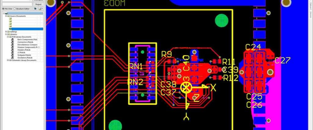
Layout – Physical board space planning, placement, substrate stackup configurations, routing, and implementation best practices.
DFMx – Applying design-for-excellence techniques for reliability, testability, manufacturing, quality, among other pillars.
CAM and Documentation – Facilitating handoffs to fabrication and assembly through comprehensive Gerbers, drawings, specifications, models, and other artifacts to enable production.
Testing – Developing testing jigs, harnesses, scripts, and measurement procedures to characterize bare boards and populated boards against specifications through validation.
Qualification – Executing rigorous process and product qualifications along with field failure analysis to instill confidence. Analyzing key metrics (MTBF, process capability indices) to quantify margins statistically.
Sustaining – Maintaining revision control, configuration management, component lifecycle roadmaps, and migration initiatives through long lifetimes from initial prototypes through sunset.
PCB engineering wear many hats! Cross-functional proficiency and attention to detail is mandatory.
PCB Materials, Technology, and Construction
At the core of PCB engineering lie the materials science and processing methods enabling fabrication of laminated boards:
Substrates – Glass reinforced epoxy laminates like FR-4 compose circuit boards providing mechanical structure. Advanced substrates boost signal speeds, thermal conductivity and precision.
Conductors – Copper foil rolled onto substrate cores patterned into signal traces, planes, and pads through photolithographic etching. Final finishes like ENIG (Gold), Imm. Ag, OSP (Organic surface protectant) coat traces.
Vias and Holes – Interlayer vertical connections between traces on layers above and below allowing routing between layers and connections to external layers.
Laminates and Stackups – Multiple layers of etched coppers and substrates pressed and glued together into multi-plane sandwich structures. Interface theming allows controlled impedances.
Soldermasks – Epoxy layers selective screen printed over copper traces as insulation, prevented unwanted bridging and enhanced appearance.
Legends – Screen/inkjet printed labels, ratings, symbols and markings onto PCBs for identification and potting prevention.
Advanced Tech – HDI processes enable dense sub 100 micron trace/spaces, buried/blind vias, and moreeeded in leading edge products.
Knowledge of these fundamental building blocks empowers innovation.
Skills and Tools
Realizing modern PCB systems requires diverse expertise:
Schematic Entry – Virtuoso, Altium, NX, PADs, Allegro, OrCAD…
PCB Layout – Altium Designer, Cadence Allegro/OrCAD, Mentor Xpedition, Zuken CR5000/CR8000…
Signal Integrity – Polar SI9000, Ansys, HFSS, Keysight ADS, Sigrity…
Power Integrity – Ansys RedHawk, Cadence Voltus, Synopsys, Silvaco…
Thermal Analysis – Finite element modeling in Ansys Flotherm, FloEFD, Mentor FloTHERM
EMI Characterization – Near field and radiated emissions tools.
Programming – Tcl, SKILL, Python, C++ custom tool automation
Domain Expertise – Materials science, manufacturing processes, interface technologies
Standards Fluency– IPC specifications, acceptability criteria
And mastering the latest high speed interfaces like DDR5, PCIe Gen 6, USB4, and more.
The breadth makes for excitingly diverse engineering careers!
Application Areas
Printed boards permeate every electronics sector as the interconnect foundation:
Consumer Electronics – Phones, laptops, gaming systems, appliances
Automotive – Engine control units, infotainment, instrument clusters
Aerospace/Defense – Avionics, weapons systems, satellites
Medical – Imaging systems, diagnostics equipment
Test and Measurement – Oscilloscopes, RF analyzers, prototyping rigs
Telecom Infrastructure – Cellular base stations, servers, routers
IoT Devices – Sensor boards, hubs, controllers
Custom Hardware – Application specific designs
And everything in between needing electronics!
Overcoming Design Challenges
Common pain points solved by PCB engineering include:
Signal Integrity – Ringing, reflections, cross-talk issues from high speed signals across backplanes. Careful topology tuning, line impedances, breakout routing mitigates problems.
Power Integrity – Simulating PDN impedances, designing sufficient decoupling for stable supplies across circuit loads.
Thermals – High component densities require understanding heat spreading materials, thermal vias, and airflow management to counter hot spots.
Miniaturization – Shrinking size constraints make stacking HDI technologies key along with strategic component arrangements.
Test Access – Designing test points, debug headers, and DFT controls facilitates characterization plus post-deployment field diagnosis.
EMI Control – Containment of radiated and conducted noise through small feature factors presents continual challenges.
And tailoring custom materials or advanced manufacturing when needed.
With increasing complexity across multiple fronts, PCB engineering strives to tame impediments through innovative problem solving.
Importance of PCBs
Why does PCB technology remain irreplaceable as the nervous system connecting and controlling electronics?
Connectivity – Interconnect electronics via copper traces in dense area arrays without manual wiring complexity
Configurability – Enable flexible schematics morphing into specialized layout arrangements through placement and routing stages tailored to product needs.
Multi-Functionality – Merge analog, digital, power, and RF subsystems together on common PCB platforms enabling highly integrated solutions.
Reliability – Mature PCB fabrication means robust, consistent electrical paths tested through harsh temperature cycling, vibration exposure and years of operation.
Serviceability – Modular subassemblies allow repair through individual replacement when faults occur during lifecycles rather than discarding entire system.
Affordability – Mature infrastructure with economies of scale make PCBs extremely cost effective and thus ubiquitous across all industries.
PCB advancements will continue driving electronics innovations through coming decades!
PCB Engineering Trends
Cutting edge developments reshaping boards include:
High Density Interconnects (HDI) – Densely integrated fine featured multilayer boards with stacked microvias enable compact system scaling.
High Speed Digital – Multi-gigabit SERDES channels remaining eye-clean using elaborately orchestrated impedance profiles, breakouts, tuning and equalization.
embedded passives – Thin film and laminate capacitors, resistors buried into boards remove discrete components.
5G mmWave Circuits – Taming lossy RF propagation above 25 GHz for phased array antenna and transceiver PCBs.
AI-enabled Engineering – Leveraging neural nets and machine learning to accelerate optimization of stackups, topology, thermal and signal integrity, reliability analysis and more.
Additive Electronics Printing – Aerosol, inkjet, extrusion and other deposition to directly 3D print passive and active components onto substrates.
Advanced Cooling Integration – Direct liquid immersion cooling channels and cold plates integrated into PCB sandwich structures for high powered computing systems.
And more nascent innovations primed to productize!
Frequently Asked Questions
Q: How are rigid-flex PCBs uniquely enabling wearable and Internet of Things designs?
A: Rigid sections provide standard component mounting while thin circtuitized flexible interconnects between enable dynamic motion range and mechanics impossible through standard rigid boards alone. Enabling game changing form factors.
Q: Which sectors most push the bleeding edge of HDI and substrate technologies?
A: Telecommunications infrastructure and networking, defense electronics, and high throughput computing data centers at the leading edge of density, layer counts, finer geometries below 25 microns.
Q: Do PCB fabricators and engineering teams need to adopt statistical process control rigors seen in adjacent industries?
A: Absolutely – especially for specialized substrates and advanced RF materials. Careful tracking and quantification of dimensional stability and passive material electrical tolerances is mandatory to achieve ±3 sigma consistency necessary to attain higher yields during volume manufacturing.
Q: How are augmented/virtual reality driving next generation embedded PCB innovation?
A: Demand for ever higher resolution displays with low latency coherent functionality is driving GPU and memory integration requiring and multi-hundred MHz signaling across dense PCB interconnects along with extensive EMI containment.
Q: Which software tools and programming languages dominate on the PCB engineering side?
Altium and Cadence feature strongly for schematic capture and layout, with a sprinkling of Mentor and Zuken users. Python leads for scripting automation, Tcl second. C++ sees selective use for custom analysis tools and cloud compute acceleration. MATLAB also remains deeply entrenched.
And there you have it – a comprehensive overview of this expansive, critically important field! PCB engineering empowers innovation across electronics like no other discipline.


0 Comments