Electronic component manufacturing represents the process of fabricating the microscopic building blocks essential for producing all modern digital products and systems. Integrated circuits, transistors, resistors and other critically enabling components undergo sophisticated technological fabrication steps before getting incorporated into finished goods.
In this comprehensive guide, we’ll explore key aspects of electronic component manufacturing like:
- Typical Components Produced
- Raw Materials Used
- Primary Fabrication Technologies
- Packaging Methods
- Production Volumes
- Quality Control Testing
Gaining familiarity with steps comprising this foundational industry assists appreciating technical underpinnings powering the trillion-dollar global electronics ecosystem. Let’s commence examining constituent components flowing through various subsector supply chains.
Electronic Components Manufactured
Hundreds of elementary constituent components classified into broad categories as outlined below become assembled creating functional printed circuit boards and modules:
Semiconductors – Integrated circuits, CPUs, memory, logic chips, etc.
Passive Components – Resistors, capacitors, inductors, transformers
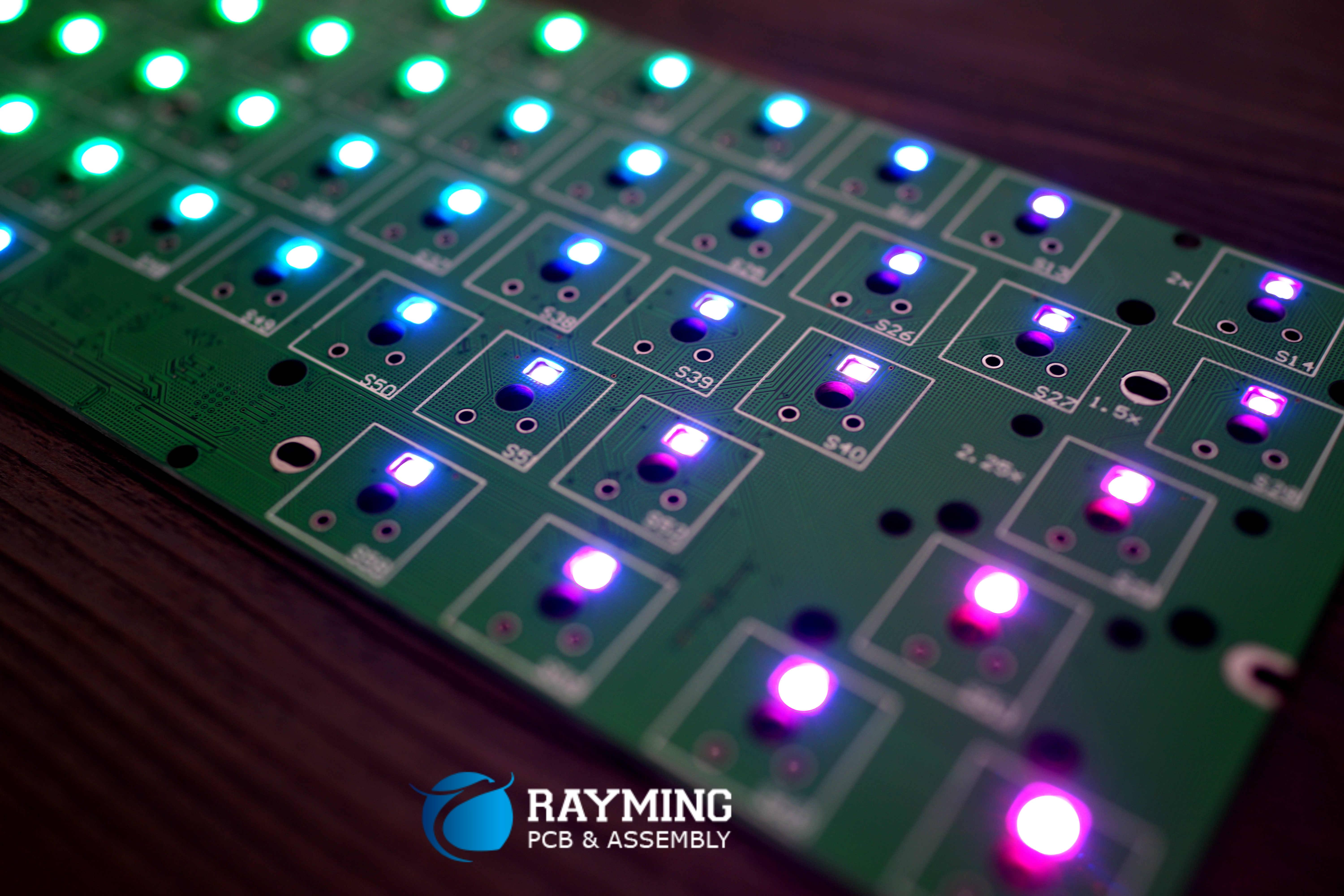
Electromechanical – Relays, switches, connectors, cables, batteries Piezoelectrics – Crystals, filters and acousticwave sensors Printed Boards – Raw PCB substrates without active components
Displays – Light emitting diodes, liquid crystals, plasma modules Microstructures – Sensors, actuators, gyros, microphones, speakers
Varying sizes from microscopic transistors to multi-inch panels span discrete media storing bits to complex logic manipulating data based on software-defined architectures implemented physically via precision manufacturing processes – the foundation underpinning all electronics innovation. Now let’s examine how raw base materials become refined and patterned into active circuitry.
Raw Materials in Electronics Manufacturing
Transcending pure metals like copper or gold, a diverse palette of elemental chemistry constitutes modern electronic components including:
Silicon – Semiconducting wafers oxidized into insulating substrates Gallium Arsenide – Alternative higher performance semiconductor Rare Earth Minerals – Specialty ceramics, crystals integrated into devices Dopants – Trace boron, phosphorus or antimony elements precisely regulating silicon conductivity
Photoresist Polymers – Light sensitive insulation layers defining etch barriers
Nanparticle Inks – Silver conductive pastes for printed electronics
Electroplating Solutions – Chemical baths depositing metallic solders and films Epoxy Resins – Adhesives encapsulating finished assemblies Organic Solvents – Cleansers removing debris between intricate process steps
Suppliers continually refine purity and consistency of these materials enabling smaller achievable geometries pushing density envelopes further. Now let’s survey this commodity transformation sequence through various process flows to construct finished components.
Electronic Component Fabrication Technologies
Constructing integrated circuits requires orchestrating collective fabrication activities including:
Wafer Processing – Grow cylindrical semiconductor crystal ingots that get sliced into pure substrate discs then meticulously altered through successive thin film deposition, photoresist patterning, chemical etching, doping, cleaning, polishing and inspection steps culminating in transistors layered side-by-side into intricate logics Housed within hardened inorganic passivation shells protecting delicate features underneath while facilitating handling and connectivity.
Die Preparation – Test functionality of patternsed wafer mosaics before segmenting individual die containing identical copies of a particular chip design freed from the wafer then ready for packaging into protective shells
Packaging Flows – Connect die terminals outwards through encapsulating package perimeter walls using fine bonding wires or dense rows of solder bumps so interior complex silicon cores route signals successfully to boards and systems ultimately destined for
Myriad machinery enables reliably generating billions of components daily encompassing simple resistors to elaborate microprocessors and flash storage chips through these collective fabrication sequences. Next let’s examine how completed bare die get further protected for shipment.
Electronic Component Packaging Techniques
Shielding vulnerable miniaturized part interiors demands effective containment strategies including:
Plastic Encapsulation – Surround silicon die with epoxy blobs or preforms molded around leads
Ceramic Housings – Enclose die inside rectangular windows framed by multilayered cofired ceramic rectangles supporting dense arrays spanning module underside
Metal Cans – Affix lids onto hollow cases soldering perimeter seals protecting interior bonded assemblies designed for rugged high performance environments
Reconstituted Wafers – Redistribute peripheral contacts inwards below die undersides using successive multilayer thin film buildup technologies allowing stacking and enhanced interconnects
Printed Structures – Screen print or inkjet protective coats, conductive traces even antennas directly onto components enhancing functionality
Conformal Coatings – Spray ultra thin polymer films preventing environmental corrosion while electrically isolating high density elements prone to shorting
Various attachment methods also permanently fix die into multichip modules combining similar or dissimilar technologies inside common packages functioning as highly integrated components for streamlining downstream production activities further.
Now let’s explore the production scale span supporting all size requirements.
Production Volumes and Batch Sizes
Fabrication facilities generate a vast range of component quantities from small prototypes to extremely high volumes:
Small Batch – Short trial builds validate designs initially generally 30-100 units
Medium Volume – Preproduction validation builds ensure repeatability around 1000+ parts
High Volume – Mature products get manufactured in much greater batches from tens of thousands to millions of units monthly
Wafer Scale – Iconic microprocessors and DRAM memory churned out in extreme numbers approaching billions annually per device type
Depending on product type and target application, this vast logarithmic quantity spectrum necessitates tailored equipment and methodologies balancing flexibility, yield rates, cycle times and costs.
But regardless of volumes, relentless quality checks persist across all flows.
Quality Control Testing
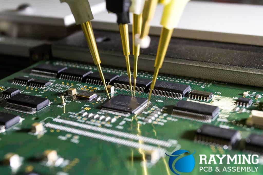
Given microscopic dimensions involved, continuous defect detection and metrology verification punctuates every step:
- Electronics building blocks undergo enormous scrutiny confirming perfect patterns precisely reproduced within each batch
- Steadily advancing inspection cameras achieve ever growing precision quantifying nanoscale variances across millions of structures hunting rare flaws
- Persistently tightening mechanical alignments maintain exacting specifications required as components shrink towards physical limits
This rigorous hyperattention towards quality stands validated statistically by continuously rising cumulative mean time between failures rates as lean six sigma controls eliminate deviations – backing reliability claims supporting safety-critical systems touching every aspect of daily lives.
With core manufacturing steps covered, let’s wrap up discussing a few frequently asked questions surrounding this foundational industry.
Electronic Component Manufacturing FAQs
What geographic regions lead production?
While pioneered in the United States originally, Taiwan and South Korea collectively produce over 60% of semiconductor output globally today trailed by North America and Europe while mainland China rapidly escalates domestic capacity aiming to eventually eclipse other territories.
What ratios split discrete versus integrated circuit categories?
Discrete diodes and transistors represent approximately 20% of components shipped annually while integrated circuits encompass the remaining 80% and should continue rising longer term as systems-on-chip consolidate additional functionality fueled by denser transistor integration.
Which specialty processes show promise for future components?
Several innovative methods hold promise for enhancing future components like multi-beam maskless photolithography, additive 3D nanoscale printing of structures, in situ doping modulation and hybrid CMOS/molecular computing architectures though fabrication challenges remain translating them to high volume manufacturing, however reliability milestones steadily approach commercial viability.
How may sustainability initiatives shape manufacturing?
Escalating environmental sensitivities surrounding semiconductor feedstock sourcing, purifications, chemistry effluents, water usage, energy budgets and workforce protections will likely impose additional constraints upon fabrication procedures placing heightened emphasis on comprehensive stewardship across production ecosystems.
In summary, meticulously orchestrating the intensely complex ballet of processes comprising electronics manufacturing demands ever advancing precision and care while manipulating nature’s foundational element itself into miraculous devices – charting this industry’s remarkable ascendency makes appreciating achievements carved into invisibly small spaces no less awe-inspiring!


0 Comments