Printed circuit boards (PCBs) serve as the backbone for interconnecting electronic components using conductive copper traces etched on an insulating substrate. PCBs undergo extensive processing to pattern the traces and drill holes for mounting components.
A mouse bite describes a particular cutout pattern purposefully incorporated along the edges between pads or traces on a PCB. Resembling the nibbling action of a mouse eating away sections, these curved shapes help mitigate stresses that arise during manufacturing and component assembly stages.
In this comprehensive guide, we dive deep on various aspects around PCB mouse bites:
Overview of Mouse Bites
Mouse bites manifest as smooth curved indentations made along PCB trace edges, pad peripheries and ground planes. The indented trace shape bites” away substrate material between adjoining conductive features. These purposeful cuts distribute mechanical stresses and prevent solder buildup issues.
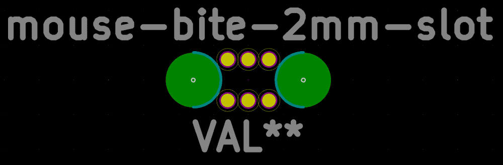
Figure 1. Mouse bites along the edge between adjacent pads
The curved smooth contour allows traces to flex and bend slightly, acting as stress relief during thermal excursions or physical manipulations. Mouse bites also channel away solder flow preventing undesired seepage between tight pitched surface mount pads.
With increasing PCB complexity and density, mouse bites provide important benefits toward defect prevention both during fabrication and component assembly.
Reasons for Using Mouse Bites
Mouse bites primarily assist in twoareas:
Mechanical Stress Relief
Printed circuit boards expand and contract with temperature fluctuations during processing like wave soldering or component mounting reflows. Shear forces develop along areas with greatly differing coefficients of thermal expansion. These manifest as cracks or delamination damage.
By incorporating mouse bites cutouts along adjoining boundary regions on a PCB, enough contour flexibility gets introduced allowing slight relative movement without shearing. The traces at these spots safely flex and bend to accommodate processing strains.
Solder Wicking Prevention
Dense surface mount pads often end up in close proximity as circuit complexity increases. During reflow soldering, excess molten solder can accumulate bridging across such narrow gaps.
Mouse bites create intentional channels along pad perimeters for outgassing and venting excess solder. This prevents solder creeping between tight pitched traces causing difficult to correct shorts. The indentations essentially guide unwanted solder away while retaining solder for the actual joint.
Figure 2. How mouse bites prevent solder bridging
These stress mitigation and solder wicking prevention benefits make mouse bites an extremely useful PCB design technique for defect reduction.
Different Mouse Bite Shapes
While all mouse bite shapes feature smooth curving cutouts to prevent crack propagation points, some varieties provide specialized advantages.
U-Shaped Mouse Bites
The U-shaped mouse bite has a rounded base with two vertical walls. It provides the highest flexibility for adjacent traces on either side to stretch without rubbing or shorting against each other. The U-contours also maximally curb solder flow between pads.
However, the indented walls reduce copper area amounting to slightly higher trace impedances. Narrow neck widths also risk etching or plating discontinuities.

Figure 3. U-shaped mouse bites between traces
V-Shaped Mouse Bites
V-shaped mouse bites do not fully surround the adjoining trace area. Instead, the partial indent leaves little copper protruding outward. This allows no wall etching issues while still reducing shearing forces through the smoother bend relief.
But solder wicking prevention becomes limited without the encompassing channel to redirect flows. Self-alignment also suffers slightly during component placement without the registration walls.
Figure 4. V-shaped mouse bite varieties
Teardrop Shaped Mouse Bites
As the name suggests, teardrop mouse bites feature rounded tapering indents as though a water droplet edge interacts with the trace. The smooth curving interface prevents stress concentrations across the entire adjacent trace boundary.
Solder wicking channels become indirect requiring deeper bite depth. But the minimal intrusion preserves optimal trace area and current handling capacity.
Figure 5. Teardrop shaped mouse bites
Here is a comparison across the popular mouse bite shapes:
| Shape | Stress Relief | Solder Prevention | Trace Impact |
|---|---|---|---|
| U-Shaped | High | Full channel | Narrow traces |
| V-Shaped | Medium | Partial | Lower copper loss |
| Teardrop | Low | Indirect | Minimizes lost area |
The choice depends on priority tradeoffs between flexibility, wicking resistance, and impedance across mounting pads.
Rules for Placement and Sizes
Certain best practices guide optimal mouse bite placement:
- Mouse bites insert at edges connecting different trace widths or pad shapes
- Cutouts stay clear of high current density areas
- Indentations remain outside solder mask openings
- Mouse bites incorporate on pads with smaller pitches (~10 mils)
- Areas between numerous adjacent pins utilize mouse bites
In terms of depth and contour sizes:
- Rounded walls maintain at least 2 mil thickness
- Maximum depth constitutes 20% pad edge
- Mouse bite radii limit under pad pitch size
-Placement stays ≥2 mils from adjacent copper
These rules prevent bites from interfering with tracing objectives while effectively promoting stress relief and solder wicking protection.
Modeling Mouse Bite Effects
The effects of mouse bites get characterized through modeling to gauge benefits versus negative impacts. Primary analyses include:
Mechanical Stress Simulation
The stresses between mouse-bitten traces when subjected to thermal or physical deflections qualify vulnerability against crack initiation and propagation. Deflection strains visualize across the junction.
Solder Spread Modeling
Wetting and surface tension physics simulate flow of solder during reflow when contacting mouse bitten pads. Spreading analysis assesses effectiveness in arresting wicking between tight spaces.
Impedance Calculations
Current flow simulations using mouse bitten trace geometries provide impedance estimates to check whether bites excessively raise inductance or resistance. Other assessments include continuity, capacitive coupling etc.
These quantifiable models help dial in optimum bite dimensions meeting design goals while preventing failure modes.
Implementation Guidelines
Standard mouse bite placement guidelines aid designers:
- Keep mouse bites ≥ 0.5 mm spacing from pad centers
- Include ~6-8 mouse bites between dense pad rows
- Place mouse bites on pad perimeter sides facing other pads
- Utilize smaller radii mouse bites for fine pitch ICs (< 0.65mm)
- Allow 0.25mm clearance between bites and solder mask
- Provide sufficient bite depth ≥ 0.3mm for wicking prevention
Maintaining clearance from joint interfaces while segmentation helps meet reliability targets.
Detection of Sub-Optimal Mouse Bites
Despite guidelines, sub-optimal mouse bite geometries still risk escaping design verification introducing field failures. Cases include:
- Insufficient bite depth unable to curb wicking flows
- Indentations encroaching excessively into current paths
- Disconnected plating inside sharp bite recesses
- Cracks from residual stress concentration points
- Excess bites weakening laminate integrity
CAM inspections, electrical testing, stress simulation, solder wick modeling help safeguard against inadequate mouse bite implementation.
Conclusion
Mouse bites describe intentional smooth indentations made along PCB trace edges adjoining pads or conductors. The curved transitions act as stress relief cuts to accommodate fabrication and assembly strains without cracking boards. Mouse bites also channel away solder during reflow preventing undesired bridging.
U-shaped, V-shaped and teardrop mouse bite varieties offer customizable blends of flexibility, wicking resistance, and minimized copper loss between adjoining pads. Controlled bite dimensions, appropriate placement, spacing rules, and modeling analysis validate balance between effectiveness and acceptable impedance/coverage impacts when preventing defects.
As a proven, low-cost PCB design technique for enhancing manufacturability and reliability, mouse bites provide an indispensable mitigation tool against increasing packaging densities and process excursions. When sanctioned judiciously following guidelines, mouse bites mechanize the vision of “fighting defects by design”.
Frequently Asked Questions
How are mouse bites useful toward PCB reliability?
Mouse bites improve reliability by:
- Allowing flexibility through intentional cuts to prevent cracks
- Venting solder creep through channels avoiding short circuits
- Mechanizing robustness against process stresses
What determines optimum mouse bite shape for a application?
Mouse bite shape depends on priorities between:
- Flexibility: U-shape has high relief
- Lost space: Teardrop preserves area
- Wicking: U-shape/V-shape channel better
Solutions come through modeling tradeoffs.
Is there an optimum number or spacing of mouse bites?
Recommended rules per product standards include:
- ~6-8 mouse bites between dense pad rows
- ≥ 0.5 mm spacing of bites from pad centers
- ≤ 20% pad edge allocation to bites
How can incorrect mouse bite implementation be detected?
Inadequate mouse bites escapes get detected through:
- Solder wicking and crack propagation simulations
- Continuity checks of plating in recesses
- Impedance, current handling evaluations
- CAM, electrical validations
What precautions apply when placing mouse bites close to solder mask openings?
Maintaining 0.25mm clearance from solder mask to mouse bites ensures:
- Sufficient mask overlap on pad edges
- Avoidance of mask sippage into recesses
- Preventing wicking traces beneath mask


0 Comments