In the world of printed circuit board (PCB) manufacturing, there are various techniques employed to create the intricate patterns and features required for electronic circuits. Among these methods, PCB milling stands out as a versatile and precise approach that offers several advantages, particularly for prototyping and low-volume production. This article delves into the concept of PCB milling, its process, applications, and benefits.
Introduction
PCB milling, also known as mechanical milling or PCB routing, is a subtractive manufacturing process that utilizes specialized computer-controlled machines to remove material from a solid substrate, typically a copper-clad board. This process enables the creation of custom PCB designs with high precision and flexibility, making it an attractive option for a wide range of applications.
What is PCB Milling?
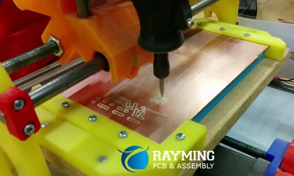
PCB milling is a manufacturing technique that involves the use of a high-speed rotating tool, known as an end mill or router bit, to selectively remove copper and substrate material from a PCB blank. The process is guided by computer-aided design (CAD) and computer-aided manufacturing (CAM) software, which translates the PCB design into precise tool paths for the milling machine to follow.
The milling process involves the following steps:
- PCB Design: The PCB design is created using specialized electronic design automation (EDA) software, resulting in gerber files or other compatible file formats.
- CAM Processing: The PCB design files are imported into CAM software, which generates the tool paths and instructions for the milling machine to follow.
- Milling Machine Setup: The PCB blank, typically a copper-clad board made of materials like FR-4 or aluminum, is securely mounted on the milling machine’s work area.
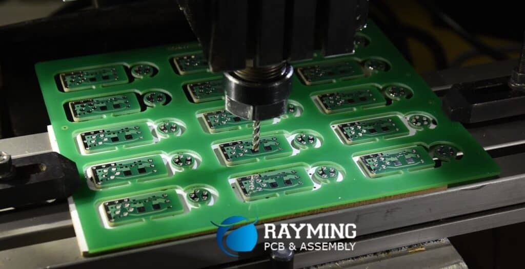
- Milling Process: The milling machine, controlled by the CAM software, moves the end mill or router bit across the PCB blank, removing copper and substrate material in the desired patterns. This process creates the traces, pads, holes, and other features required for the PCB design.
- Post-Processing: After milling, additional processes such as cleaning, drilling, and surface finishing may be performed to prepare the PCB for component assembly or further processing.
Advantages of PCB Milling
PCB milling offers several advantages over other PCB manufacturing methods, making it a popular choice for various applications:
- Flexibility: PCB milling allows for the creation of highly customized and complex PCB designs with ease, enabling rapid prototyping and design iterations.
- Precision: The computer-controlled milling process ensures high precision and accuracy, allowing for the creation of intricate features and fine-pitch components.
- Material Compatibility: PCB milling can be performed on a wide range of materials, including different types of copper-clad boards, aluminum, and even non-conductive substrates like plastic or wood.
- Quick Turnaround: Compared to traditional PCB manufacturing methods, PCB milling can provide faster turnaround times, particularly for low-volume or prototyping projects.
- Cost-Effectiveness: For small production runs or prototyping, PCB milling can be more cost-effective than traditional manufacturing methods, as it does not require the creation of expensive tooling or photolithography processes.
- Design Iterations: The ability to quickly modify and update PCB designs makes PCB milling ideal for iterative prototyping and testing, allowing for rapid design improvements and optimizations.
Applications of PCB Milling
PCB milling finds applications across various industries and sectors, including:
- Prototyping and Product Development: PCB milling is widely used in the prototyping and product development phases of electronic devices, enabling rapid design iterations and testing.
- Research and Education: In academic and research settings, PCB milling provides a cost-effective and accessible means for creating custom PCBs for experimental projects and educational purposes.
- Low-Volume Production: For small-scale production runs or specialized applications, PCB milling offers a viable alternative to traditional manufacturing methods, allowing for quick turnaround times and cost-effective production.
- Hobbyists and DIY Projects: The accessibility and versatility of PCB milling have made it popular among hobbyists, makers, and DIY enthusiasts for creating custom PCBs for their projects.
- Aerospace and Defense: In the aerospace and defense industries, PCB milling is utilized for prototyping and low-volume production of specialized electronics, where precision and flexibility are crucial.
- Automotive and Transportation: The automotive and transportation sectors leverage PCB milling for prototyping and low-volume production of various electronic systems, such as control modules and sensor boards.
Design Considerations for PCB Milling
While PCB milling offers numerous advantages, there are several design considerations to keep in mind:
- Feature Size Limitations: Due to the physical size of the milling tools, there are limitations on the smallest feature sizes and trace widths that can be achieved. Designs requiring extremely fine-pitch components or intricate features may not be suitable for PCB milling.
- Material Thickness: The thickness of the PCB material can impact the milling process and the achievable precision. Thicker materials may require specialized tooling or multiple passes, potentially increasing manufacturing time and cost.
- Tool Selection: Choosing the appropriate milling tool (end mill or router bit) is crucial for achieving the desired feature quality and surface finish. The tool’s diameter, material, and cutting geometry play a significant role in the milling process.
- Tool Wear and Replacement: Milling tools are subject to wear and tear, which can affect the quality of the milled features over time. Regular tool inspection and replacement may be necessary to maintain consistent quality.
- Surface Finish: While PCB milling can produce high-quality surface finishes, additional post-processing steps, such as sanding or polishing, may be required to achieve desired surface smoothness or aesthetic requirements.
- Electrical Properties: The milling process can potentially affect the electrical properties of the PCB, such as impedance and signal integrity, particularly for high-frequency or sensitive applications. Proper design considerations and post-processing steps may be necessary to mitigate these effects.
Frequently Asked Questions (FAQs)
- Q: How does PCB milling compare to traditional PCB manufacturing methods in terms of cost and lead time? A: For low-volume or prototyping projects, PCB milling can be more cost-effective and have shorter lead times compared to traditional methods like photolithography and chemical etching. However, for high-volume production, traditional methods may be more economical.
- Q: Can PCB milling be used for multi-layer PCB designs? A: Yes, PCB milling can be used to create multi-layer PCB designs, but the process may involve additional steps, such as lamination or stacking of individual milled layers.
- Q: What are the typical materials used for PCB milling? A: Common materials used for PCB milling include copper-clad FR-4 boards, aluminum, and other conductive or non-conductive substrates like plastic or wood, depending on the application.
- Q: Can PCB milling be automated for higher production volumes? A: While PCB milling is often associated with low-volume or prototyping applications, it can be automated and scaled for higher production volumes using specialized milling machines and workflows.
- Q: How does the surface finish of a milled PCB compare to traditional PCB manufacturing methods? A: PCB milling can produce high-quality surface finishes, but additional post-processing steps may be required to achieve the desired smoothness or aesthetic requirements, particularly for demanding applications.
PCB milling has emerged as a versatile and valuable manufacturing technique in the electronics industry, offering flexibility, precision, and cost-effectiveness for prototyping, low-volume production, and specialized applications. With its ability to create custom PCB designs rapidly and accommodate a wide range of materials, PCB milling has become an essential tool for designers, engineers, and manufacturers alike. As technology continues to evolve, PCB milling will undoubtedly continue to play a pivotal role in driving innovation and enabling the creation of cutting-edge electronic devices and systems.


0 Comments