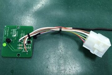
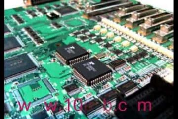
What is PCB Copper Layers

Understanding PCB Copper Layers What are PCB Copper Layers? PCB copper layers are thin sheets of copper foil laminated onto the surface of a non-conductive substrate, typically made of fiberglass or other materials. These copper layers form the conductive pathways that allow electrical signals to travel between components on the Read more…

What is a Microvia?

Microvia Definition A microvia is a small, laser-drilled hole that connects the outer layer of a printed circuit board (PCB) to the inner layers. These tiny vias are essential for high-density interconnect (HDI) PCBs, which are used in various electronic devices, such as smartphones, tablets, and laptops. Microvias enable the Read more…

What is a Multi-Layer PCB?

Introduction to Multi-Layer PCBs A Multi-Layer PCB, or Multi-Layer Printed Circuit Board, is a complex type of circuit board that consists of multiple layers of conductive copper foil laminated together with insulating material. These layers are interconnected through a series of drilled holes called vias, which allow electrical signals to Read more…

What is an Annular Ring?

The Importance of Annular Rings in PCB Design Mechanical Stability Annular rings provide mechanical stability to the components mounted on a PCB. They help to distribute the stress and strain caused by the insertion and removal of components, as well as the thermal expansion and contraction during operation. Without adequate Read more…

What is a PCB Substrate?

Understanding PCB Substrates A PCB substrate is the insulating material that forms the base of a printed circuit board. It provides a stable and non-conductive surface for the copper traces and components to be placed on. The substrate also plays a vital role in determining the overall performance and reliability Read more…