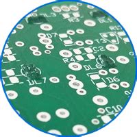
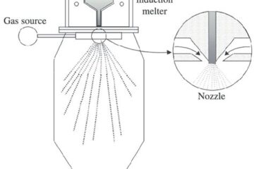
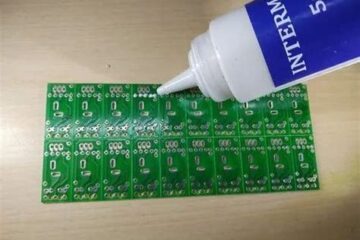
Software to panelize PCB

Introduction to PCB Panelization PCB panelization is the process of combining multiple printed circuit board designs onto a single panel for manufacturing. This technique is widely used in the electronics industry to optimize production efficiency and reduce costs. By grouping multiple PCBs together, manufacturers can minimize material waste, streamline the Read more…

Ten Common problems in PCB Design

Introduction to PCB Design Issues Printed Circuit Board (PCB) design is a complex process that requires careful consideration of various factors to ensure optimal performance, reliability, and manufacturability. Despite the advancements in PCB design software and manufacturing techniques, designers often encounter numerous challenges that can lead to costly mistakes and Read more…

How A 3 Layer PCB Is Stacked Up

What is a PCB Stackup? A PCB (Printed Circuit Board) stackup refers to the arrangement of copper layers and insulating materials that make up a printed circuit board. It is a critical aspect of PCB design, as it determines the board’s electrical properties, signal integrity, and manufacturability. A well-designed stackup Read more…

What is Halogen Free PCB

Introduction to Halogen-free PCBs Printed Circuit Boards (PCBs) are essential components in modern electronics, providing a platform for interconnecting various electronic components. As technology advances and environmental concerns grow, the demand for safer and more Eco-Friendly PCBs has increased. One such development is the introduction of halogen-free PCBs, which have Read more…

Why PCBs are green

Introduction to PCBs and Their Environmental Impact Printed Circuit Boards (PCBs) are essential components in almost all modern electronic devices, from smartphones and computers to medical equipment and automotive systems. While PCBs have revolutionized the electronics industry, their production and disposal have raised concerns about their environmental impact. However, recent Read more…