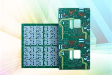
PCBA
Top Factors to Consider for Selection of PCB Supplier!
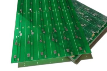
Understanding Your PCB Requirements Before diving into the selection process, it is essential to have a clear understanding of your PCB requirements. This includes factors such as: PCB Type and Complexity PCBs come in various types and complexity levels, such as: Single-sided PCBs Double-sided PCBs Multi-layer PCBs Flexible PCBs Rigid-flex PCBs Determine the type and complexity of the PCB that best suits your project requirements. PCB Material and Specifications Consider the material and specifications needed Read more…