PCBA
Flexible PCB Manufacturers in China
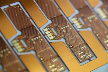
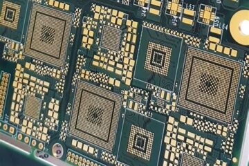
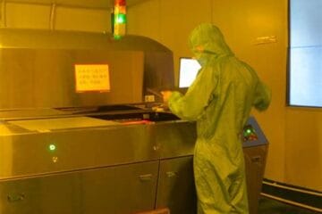
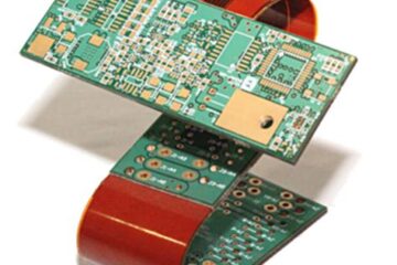
Introduction to Flexible PCBs Flexible printed circuit boards (PCBs) have revolutionized the electronics industry with their versatility, durability, and space-saving design. Unlike traditional rigid PCBs, flexible PCBs can bend, twist, and conform to various shapes, making them ideal for applications that require flexibility and compact packaging. With the increasing demand for smaller, lighter, and more adaptable electronic devices, the market for flexible PCBs has grown significantly, and China has emerged as a leading player in Read more…