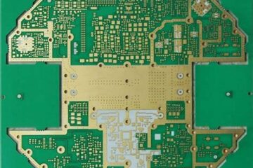
PCBA
LED CIRCUIT BOARDS
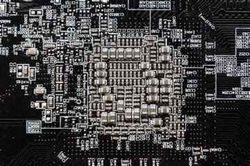
What are LED-PCBs? LED-PCBs, or Light Emitting Diode Printed Circuit Boards, are specialized circuit boards designed to power and control LED lights. These boards are essential components in a wide range of applications, from simple indicator lights to complex LED displays and lighting systems. LED-PCBs are composed of a non-conductive substrate, typically made of fiberglass or other composite materials, with conductive copper traces printed on the surface. These traces connect various electronic components, such as Read more…