PCBA
Choose reliable Rigid flex PCB manufacturer to meet your Industry Demand!
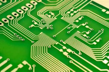
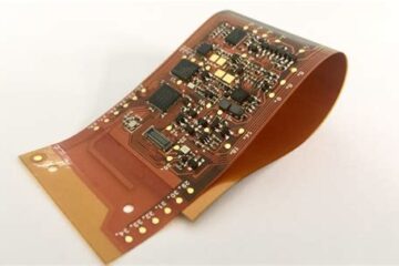
Introduction to Rigid-flex PCBs Rigid-flex PCBs are a unique type of printed circuit board that combines the stability and durability of rigid PCBs with the flexibility and versatility of flexible PCBs. This combination allows for more compact and efficient designs in various industries, including aerospace, medical devices, automotive, and consumer electronics. As the demand for smaller, lighter, and more reliable electronic devices grows, the importance of choosing a reliable rigid-flex PCB manufacturer becomes increasingly crucial. Read more…