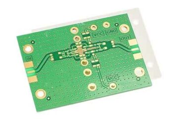
PCBA
Best Practice for PCB Moisture Protection in Outdoor Environments
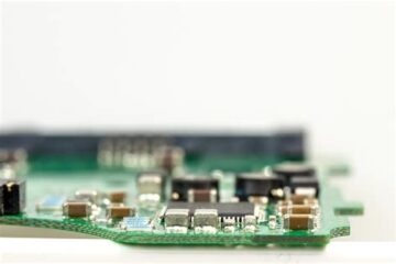
Understanding the Effects of Moisture on PCBs Moisture can have several detrimental effects on PCBs: Corrosion: When exposed to moisture, the metal components on a PCB can corrode, leading to reduced conductivity and potential short circuits. Delamination: Moisture can cause the layers of a PCB to separate, resulting in delamination and compromised structural integrity. Electromigration: High humidity levels can accelerate electromigration, causing the movement of metal ions and potentially leading to open circuits. Fungal Growth: Read more…