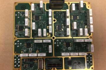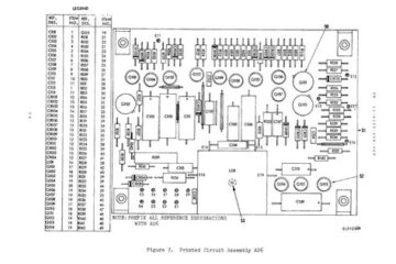
PCBA
High-speed PCB Design – 4 Things That are Very Helpful to You
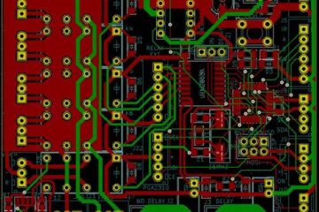
Understanding the Basics of High-speed PCB Design Before delving into the specific techniques, it’s essential to understand the fundamentals of high-speed PCB design. High-speed signals are typically defined as those with rise times less than 1 nanosecond or frequencies above 100 MHz. At these speeds, the behavior of the signals becomes more complex, and designers must consider factors such as impedance matching, signal integrity, and electromagnetic interference (EMI). Key Concepts in High-speed PCB Design Impedance Read more…